0.35
µ
µ
µ
µ
m 8-BIT 30MSPS ADC
BW1237X
1
GENERAL DESCRIPTION
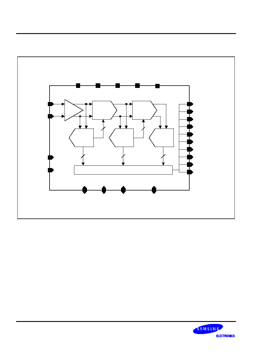
The BW1237X is a CMOS 8-bit A/D converter for video applications. It is a three-stage pipelined A/D converter
which consists of sample-and-hold circuit, two multiplying DACs, and three flash ADCs.
The maximum conversion rate of BW1237X is 30MSPS and supply voltage is 2.0V single.
TYPICAL APPLICATIONS
-- Multi-media applications
-- Frame-grabber scanner
-- Camcorder
-- Digital video (TV/VCR)
-- Broadcasting and studio equipments.
-- Medical Electronics (ultra-sound and imaging)
-- High speed instruments (Digital scope, radar)
FEATURES
-- Process: CMOS
-- Resolution: 8Bit
-- Maximum Conversion Rate: 30MSPS
-- Power Supply: 2.0V Single
-- Power Consumption: 40mW
-- Differential Linearity Error: ¡¾0.8 LSB(Typ)
-- Integral Linearity Error: ¡¾1.0 LSB(Typ)
-- Sample and Hold Function Implemented
0.35
µ
µ
µ
µ
m 8-BIT 30MSPS ADC
BW1237X
3
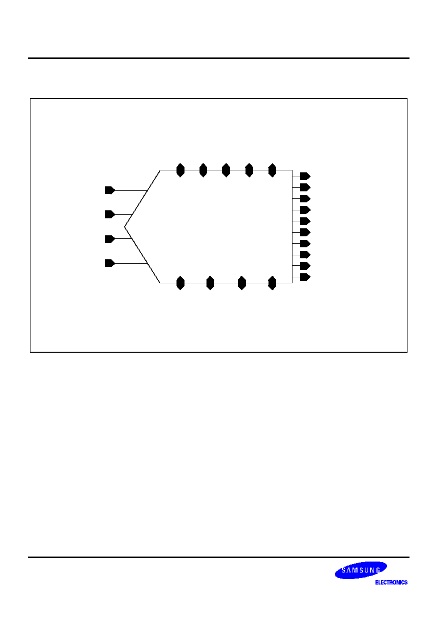
CORE PIN DESCRIPTION
Name
I/O Type
I/O PAD
Pin Description
REFT
AB
poa_bb
+1.1V Reference Top Bias.
REFB
AB
poa_bb
+0.5V Reference Bottom Bias.
CML
AB
poa_bb
Internal Bias (Test Pin).
VDDA
AP
vdda
+2.0V Analog Power.
VBB
AG
vbba
Sub Bias.
VSSA
AG
vssa
Analog Ground.
AINT
AI
piar10_bb
Analog Input.
Input Span : 0.0V ~ 1.2V
AINC
AI
piar10_bb
Analog Input.
Input : Analog Ground
ITEST
AB
poa_bb
Open (Use Internal Bias)
STBY
DI
picc_bb
High (Power Saving Standby Mode)
Low (Normal Operation)
CLK
DI
picc_bb
Clock Input.
DO[7:0]
DO
pot2_bb
Digital Output.
UDF
DO
pot2_bb
UnderFlow Indication.
OVF
DO
pot2_bb
OverFlow Indication.
VSSD
DG
vssd
Digital Ground.
VDDD
DP
vddd
+2.0V Digital Power.
I/O Type Abbr.
-- AI: Analog Input
-- DI: Digital Input
-- AO: Analog Output
-- DO: Digital Output
-- AB: Analog Bidirectional
-- DB: Digital Bidirectional
-- AP: Analog Power
-- DP: Digital Power
-- AG: Analog Ground
-- DG: Digital Ground

0.35
µ
µ
µ
µ
m 8-BIT 30MSPS ADC
BW1237X
5
ABSOLUTE MAXIMUM RATINGS
Characteristics
Symbol
Value
Unit
Supply Voltage
VDD
-0.3 to 4.5
V
Analog Input Voltage
AINT
-0.3 to VDD+0.3
V
Digital Input Voltage
CLK
-0.3 to VDD+0.3
V
Digital Output Voltage
V
OH
, V
OL
-0.3 to VDD+0.3
V
Reference Voltage
REFT/REFB
-0.3 to VDD+0.3
V
Storage Temperature Range
T
stg
-45 to 125
°
C
NOTES:
1.
ABSOLUTE
MAXIMUM
RATING
specifies
the
values
beyond
which
the
device
may
be
damaged
permanently.
Exposure
to
ABSOLUTE
MAXIMUM
RATING
conditions
for
extended
periods
may
affect
reliability.
Each
condition
value
is
applied
with
the
other
values
kept
within
the
following
operating
conditions
and
function
operation
under
any
of
these
conditions
is
not
implied.
2.
All
voltages
are
measured
with
respect
to
VSS
unless
otherwise
specified.
3.
100pF
capacitor
is
discharged
through
a
1.5K
resistor
(Human
body
model)
RECOMMENDED OPERATING CONDITIONS
Characteristics
Symbol
Min
Typ
Max
Unit
Supply Voltage
VDDA - VSSA
VDDD - VSSD
1.9
2.0
2.1
V
Supply Voltage Difference
VDDA - VDDD
-0.1
0.0
0.1
V
Reference Input Voltage
REFT
REFB
1.1
0.5
V
Analog Input Voltage Positive Port
AINT
0.0
1.2
V
Analog Input Voltage Negative Port
AINC
0.0
V
Operating Temperature
T
opr
0
70
°
C
NOTE: It
is
strongly
recommended
that
all
the
supply
pins
(VDDA,
VDDD,
VDDP)
be
powered
from
the
same
source
to
avoid
power
latch-up.