0.35
µ
µ
µ
µ
m 3.3 V 8-BIT 3MSPS DAC
BW1245X
1
GENERAL DESCRIPTION
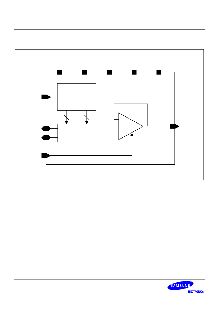
The BW1245X is a CMOS 8-bit D/A converter for general applications. It consists of a 1-of-256 decoder, a resistor
string with 256 resistors and an OP amp block.
The maximum conversion rate of BW1245X is 3MSPS and supply voltage is 3.3V single.
TYPICAL APPLICATIONS
-- Hard Disk Drive (HDD)
-- Battery Operated Instruments
-- Motor Control Systems
-- General Applications
FEATURES
-- Resolution : 8Bit
-- Differential Linearity Error : ± 0.5 LSB
-- Integral Linearity Error : ± 1.0 LSB
-- Maximum Conversion Rate : 3MSPS
-- Low Power Consumption : 9.9mW
-- Power Down Mode
-- Operation Temperature Range : 0ºC ~ 70ºC
-- Power Supply : 3.3V Single
0.35
µ
µ
µ
µ
m 3.3 V 8-BIT 3MSPS DAC
BW1245X
3
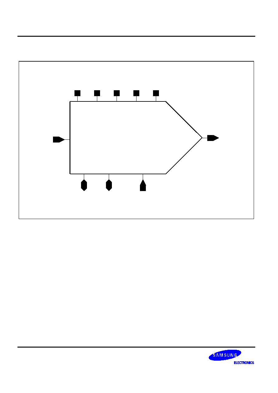
CORE PIN DESCRIPTION
Name
I/O Type
I/O Pad
Pin Description
D[7:0]
DI
picc_bb
Digital Input Data (8BIT)
D[7] : MSB , D[0] : LSB
PWDN
DI
picc_bb
Power Down (Active Low)
VRT
AB
pia_bb
Voltage Reference Top
VRB
AB
pia_bb
Voltage Reference Bottom
VOUT
AO
poa_bb
Analog Voltage Output
VDDD
DP
vddd
Digital Power (+3.3V)
VSSA
DG
vssd
Digital Ground (0.0V)
VDDA
AP
vdda
Analog Power (+3.3V)
VSSA
AG
vssa
Analog Ground (0.0V)
VBBA
AG
vbba
Analog Sub Bias (0.0V)
I/O Type Abbr.
-- AI: Analog Input
-- DI: Digital Input
-- AO: Analog Output
-- DO: Digital Output
-- AB: Analog Bidirectional
-- DB: Digital Bidirectional
-- AP: Analog Power
-- DP: Digital Power
-- AG: Analog Ground
-- DG: Digital Ground
0.35
µ
µ
µ
µ
m 3.3 V 8-BIT 3MSPS DAC
BW1245X
5
ABSOLUTE MAXIMUM RATINGS
Characteristics
Symbol
Value
Unit
Supply Voltage
VDD (VDDA,VDDD)
4.5
V
Analog Output Voltage
VOUT
VSS to VDD
V
Digital Input Voltage
D[7:0]
VSS to VDD
V
Reference Voltage
VRT
VRB
VDD
VSS
V
Operating Temperature Range
Topr
0 to 70
°C
NOTES :
1.
ABSOLUTE MAXIMUM RATING specifies the values beyond which the device may be damaged permanently.
Exposure to ABSOLUTE MAXIMUM RATING conditions for extended periods may affect reliability. Each condition
value is applied with the other values kept within the following operating conditions and function operation under any
of these conditions is not implied.
2.
All voltages are measured with respect to VSS(VSSA or VSSD or VBBA) unless otherwise specified.
3.
100pF capacitor is discharged through a 1.5k
resistor (Human body model)
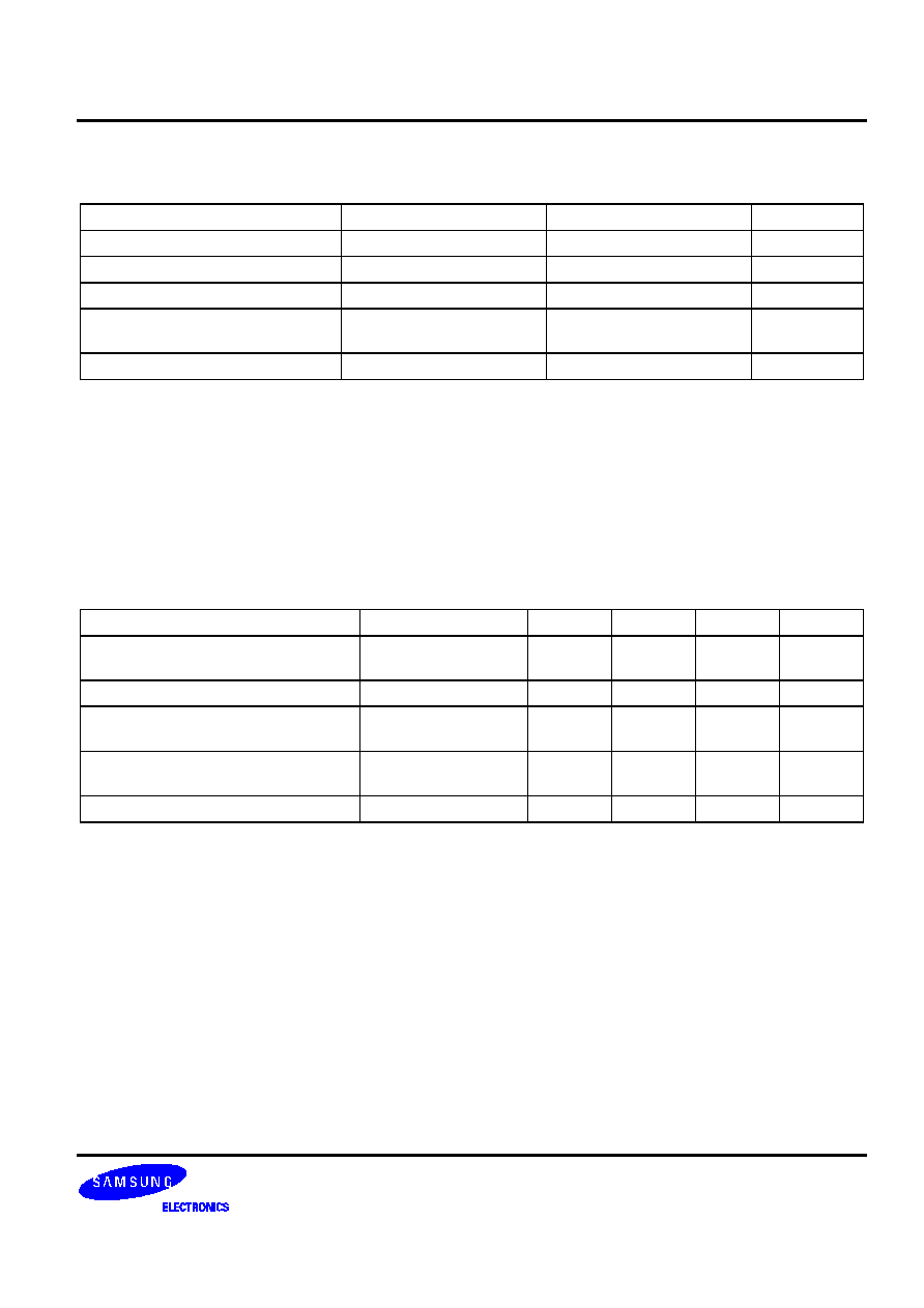
RECOMMENDED OPERATING CONDITIONS
Characteristics
Symbol
Min
Typ
Max
Unit
Supply Voltage
VDDA - VSSA
VDDD - VSSD
3.15
3.3
3.45
V
Supply Voltage Difference
VDDA - VDDD
-0.1
0.0
0.1
V
Reference Voltage
VRT
VRB
-
0.0
-
-
3.3
-
V
Digital Input 'Low' Voltage
Digital Input 'High' Voltage
VIL
VIH
-
0.7´VDD
-
-
0.3´VDD
-
V
Operating Temperature
Topr
0
-
70
°C
NOTE: It is strongly recommended that to avoid power latch-up all the supply pins(VDDA,VDDD) be driven from the same
source.