 | –≠–ª–µ–∫—Ç—Ä–æ–Ω–Ω—ã–π –∫–æ–º–ø–æ–Ω–µ–Ω—Ç: bw1249x | –°–∫–∞—á–∞—Ç—å:  PDF PDF  ZIP ZIP |
This chip is a CMOS triple 14bit D/A
converter for general & video applications.
Its maximum conversion rate is 40MSPS
and supply voltage is 3.3V single. An
external(optional) or internal 1.24V reference
voltage(VREF) and a single external resister
control the full-scale output current.
It uses the two architecture of current-
segment and binerary-weighted.
* 40MSPS 1clock pipeline delay operation(Typ)
* +3.3V CMOS monolithic construction
*
±
2.5LSB differential linearity (Typ)
*
±
5.0LSB integral linearity (Typ)
* External or internal voltage reference
(Including Band Gap Reference Block)
* Single Channel DAC
* 14-Bit parallel Digital input per channel
* High impedance differential current output
* Binary coding input
* High impedance analog output current
source
* Temperature : 0 ~ 70
∞
C
* Power_Down
FEATURES
TYPICAL APPLICATION
*High Definition Television(DTV,HDD)
*High Resolution Color Graphics
*Hard Disk Driver
*CAE/CAD/CAM
*U_ADSL
*Image Processing
*Instrumentation
*Conventional Digital to Analog
Conversion
GENERAL DESCRIPTION
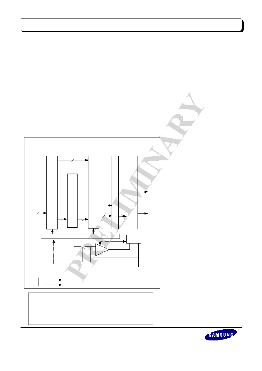
FUNCTIONAL BLOCK DIAGRAM
Ver 1.1 (Feb. 2000)
This datasheet is a preliminary version. No responsibility is
assumed by SEC for its use nor for any infringements of patents
or other rights of third parties that may result from its use. The
content of this datasheet is subject to change without any notice.
CLKGEN
CLK
COMP
OPA
CM
IREF
V
R
E
F
F
i
r
s
t
L
a
t
c
h
S
W
I
T
C
H
D
e
c
o
e
d
e
r
IO
DIN[13:0]
BGR
P
D
B
G
R
S
W
14
6
63
S
e
c
o
n
d
L
a
t
c
h
71
P
D
_
C
N
T
R
L
71
*
: Signal Flow
*
: Power_Down Control Flow
8
IOB
1 / 11
14BIT 40MSPS SINGLE DAC
BW1249X
SAMSUNG ELECTRONICS Co. LTD
SEC ASIC
BW1249X
14BIT 40MSPS Single DAC
ANALOG
NAME
I/O
TYPE
I/O PAD
PIN DESCRIPTION
PD
DI
picc_bb
Power Down
(high enable)
DIN[13:0]
DI
picc_bb
Digital input
VDDD
DP
vdd3t_bb
Digital Power
VDDA
AP
vdd3t_bb
Analog Power
VSSD
DG
vsst_bb
Digital Ground
VSSA
AG
vsst_bb
Analog Ground
VBB
AG
vbb_bb
Substrate Bias
CLK
DI
picc_bb
Clock Input
BGRSW
AI
pia_bb
Reference Voltage selecting signal
IO
AO
poa_bb
Positive Analog Current Output
IOB
AO
pop_bb
Negative Analog Current Output
VREF
AI
pia_bb
External Reference voltage
IREF
AI
pia_bb
External resistor connection
COMP
AO
pia_bb
External capacitance connection
PIN CONFIGURATION
I/O TYPE ABBR.
- AI : Analog Input
- DI : Digital Input
- AO : Analog Output
- DO : Analog Output
- AP : Analog Power
- AG : Analog Ground
- DP : Digital Power
- DG : Digital Ground
- AB : Analog Bidirectional
- DB : Digital Bidirectional
CORE CONFIGURATION
bw1249x
DIN[13:0]
IO
P D
V R E F
B G R S W
C O MP
I R E F
C L K
VBB
VDDD
VSSD
VDDA
VSSA
IOB
2 / 11
SEC ASIC
BW1249X
14BIT 40MSPS Single DAC
ANALOG
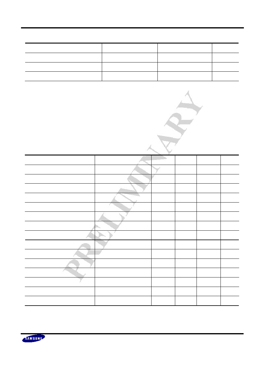
CHARACTERISTIC
SYMBOL
VALUE
UNIT
Supply Voltage
VDDD,VDDA
5.0
V
Voltage on Any Digital Pin
Vin
VSSD-0.3 to VDDD+0.3
V
Storage Temperature Range
Tstg
-45 ~ 125
∞
C
NOTES
1. ABSOLUTE MAXIMUM RATING specifies the values beyond which the device may be damaged
permanently.
Exposure to ABSOLUTE MAXIMUM RATING conditions for extended periods
may affect reliability. Each condition value is applied with the other values kept within the following
operating conditions and function operation under any of these conditions is not implied.
2. All voltages are measured with respect to GND unless otherwise specified
3. Applied voltage must be limited to specified range.
NOTES
1. It is strongly recommended that all the supply pins (VDDA,VDDD)
be powered from the same source avoid power latch-up.
CHARACTERISTICS
SYMBOL
MIN
TYP
MAX
UNIT
Operating Supply Voltage
VDDD,VDDA
3.15
3.3
3.45
V
Digital Input Voltage High
V
IH
0.7VDDD
3.3
-
V
Digital Input Voltage Low
V
IL
-
0.0
0.3VDDD
V
Operating Temperature Range
Topr
0
25
70
∞
C
Output Load(effective)
R
L
-
37.5
-
Reference Load(effective) Resistor
Rset
-
1240
-
Reference Voltage
V
REF
-
1.24
-
V
Data Input Setup Time
T
S
-
1.5
2
ns
Data Input Hold Time
T
H
-
1.5
2
ns
Clock Cycle Time
T
CLK
25
-
-
ns
Clock Pulse Width High
T
PWH
12
-
-
ns
Clock Pulse Width Low
T
PWL
12
-
-
ns
Low(Zero Level) Offset Voltage
V
off-l
-10
0
+10
mV
High(Top Level) Offset Voltage
V
off-h
-100
0
+100
mV
IREF Current
I
REF
950
1000
1050
uA
ABSOLUTE MAXIMUM RATINGS
RECOMMENDED OPERATING CONDITIONS
3 / 11
SEC ASIC
BW1249X
14BIT 40MSPS Single DAC
ANALOG
DC ELECTRICAL CHARACTERISTICS
AC ELECTRICAL CHARACTERISTICS
NOTE:
∑ The above parameters are not tested through the temperature range, but these are guaranted
over the full temperature range.
∑ Clock & data feedthrough is a function of the amount of overshoot and undershoot on the digital inputs.
∑ Settling time does not include clock and data feedthrough . Glitch impulse include clock and data feedthrough.
NOTES
1. Converter Specifications (unless otherwise specified)
VDDA=VDDD=3.3V VSSA=VSSD=GND Ta=25
∞
C Rset=1240
R
io
=R
iob
=37.5
Vref=1.24V C
COMP
=0.1
µ
F
2. TBD : To Be Determined
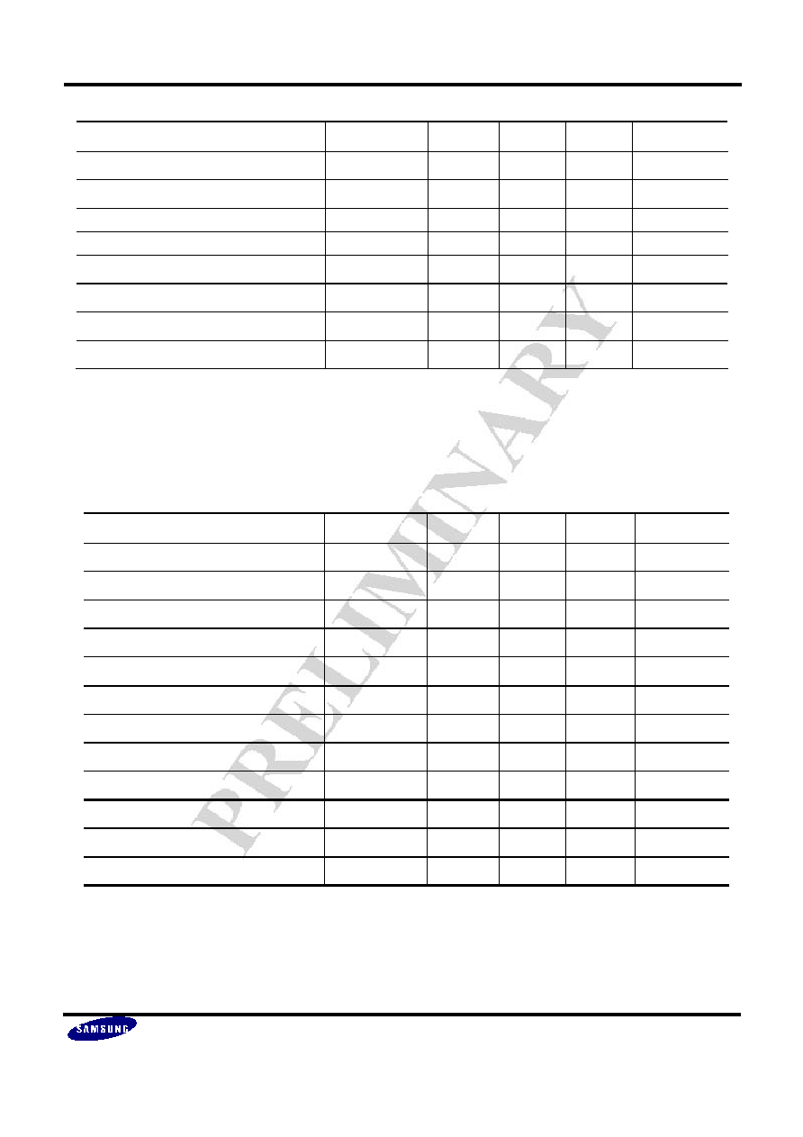
Characteristics
Symbol
Min
Typ
Max
Unit
Resolution
-
-
12
-
Bits
Full Scale Current(single)
I
fs
23
27
31
mA
Differential Linearity Error
DLE
-
2.5
TBD
LSB
Integral Linearity Error
ILE
-
±
5.0
TBD
LSB
LSB Size(single)
-
-
±
1.63
-
µ
A
Output Compliance(single)
V
OC
-0.3
0.0
+1.1
V
External Reference Voltage
V
REF
-
1.24
-
V
Supply Current at Power_Down
Ispda
-
300
-
µ
A
Characteristics
Symbol
Min
Typ
Max
Unit
Power_Down on Time per channel
Tpn
-
30
-
ns
Power_Down off Time per channel
Tpf
-
2.5
-
ms
Power Supply Rejection Ratio
PSRR
-20
-45
-
dB
Clock Rate
F
MAX
-
20
40
MHz
Analog Output Delay
Td
-
-
15
ns
Analog Output Rise Time
Tr
-
-
5
ns
Analog Output Fall Time
Tf
-
-
5
ns
Analog Output Settling Time
Tset
-
-
200
ns
Clock & Data Feedthrough
FDTHR
-
-25
-20
dB
Glitch Impulse
Gl
-
±
120
±
300
pv*sec
Pipeline Delay
Top
-
1
-
CLKs
Supply Current
Is
-
-
40
mA
4 / 11

SEC ASIC
BW1249X
14BIT 40MSPS Single DAC
ANALOG
FUNCTIONAL DESCRIPTION
The digtal input data are buffered in 1st Latch block and 6 MSBs are divided into 63
thermometer codes in Decoder block with 8LSBs are delayed in delay cell to reduce
hold_time & setup-time by adjusting the delay
same with Decoder block. Finally the 71
digital codes(63 thermometer codes & 8 delayed LSB codes) are synchronized in 2nd Latch
block. Each 63 thermometer code data drives analog switch that connected with 31-current
sources. The 8 LSB data drive analog switch that connected with binary weighted current
source mapping to each bit. Current segmented architecture DAC has analog switch composed
of source coupled pair for high conversion speed and differential output. The voltage output
is gained by summing the currents derived from current switches and letting the currents
flow through the enternal resistative loads(Rio, Riob). To provide a refernce current to
reference current mirror block, the DAC needs a resistor and an voltage reference which can
be gained by external voltage source or internal Band Gap Reference(BGR) block. This is
triple 14bit 40MSPS digital to analog data converter and uses current-segment architecture for
6bits of MSB sides and binerary-weighted architecture for 8bits of LSB side. It contains of
1st latch block, decoder block, 2nd latch block, OPA block, CM(current mirror)block
,BGR(Band Gap Reference) block and analog switch block, etc. This core uses reference
current which decide the 1LSB current by dividing the reference current by 76 times. So the
reference current must be constant and it can be constant by using OPA block with high DC
gain. The most significant block is analog switch block and it must maintain the uniformity
at each switch, so layout designer must care of it. And more than 80% of supply current is
dissipated at analog switch block. And it uses samsung standard cell(std90) as all digital cell
of latch, decoder and buffer, etc. And to adjust full current output range, you must decide
the Rset value(connected to IREF pin) and Vref voltage value(connected to VREF pin). Its
voltage output can be obtained by connecting R
io
(connected to IO pin) and Riob(connected to
IOB pin). So the differential voltage output is reauired by substrating Viob from Vio. Its
maximum differential output voltage limit is about 2.0V. So you must decide the R
io
, R
iob
,
Vbias and Rset carefully not to
exceed the output voltage limit. It contains PD pin for
saving the power-consumption by stopping this core's operating when not used. If PD input
is high, then all blocks of this core are disable, so at this case supply current is almost only
the sum of leakage_less than 300uA). You can use internal BGR output as Vbias voltage. If
you want to use that, make the BGRSW pin low and you can check the BGR's output
voltage by measuring and checking the VREF pin.
5 / 11
SEC ASIC
BW1249X
14BIT 40MSPS Single DAC
ANALOG
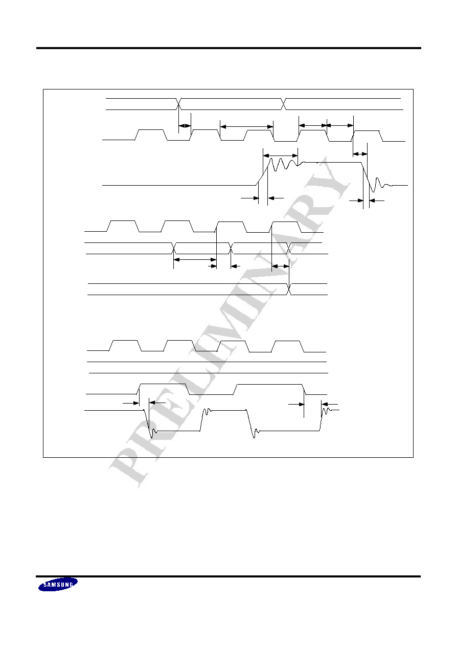
TIMING DIAGRAM
NOTES:
∑ The Behavioral Modeling is provided by Verilog HDL modeling file which includes the spec of
pipeline delay, setup_time, hold_time, rising time, falling time, and clock frequency, and so on.
∑ Output delay(Td) measured from the 50% point of the rising edge of CLK to the full scale trasition
∑ Settling time(Tset) measured from the 50% point of full scale transition to the output remaining
within
±
1LSB.
∑ Output rising(Tr)/falling(Tf) time measured between the 10% and 90% points of full scale transition.
∑ Any power_down doesn't need clock signal.
V
DOUT
CLK
DIN[13:0]
1 Clocks Pipeline Delay
data(111111111111111111)
000000000000000000
t
R
Ts
Tpwh
Tpwl
000000000000000000
Tclk
Tset
t
F
Td
High
Low
Vdout(peak)
Vdout(low)
CLK
Ts
Th
Td
DIN[13:0]
data[2]
data[3]
data[1]
V
DOUT
Vout[2]
Vout[1]
CLK
DIN[13:0]
data1(111111111111111111)
IO
PD
Tpn
Tpf
0V
Vout(pp)
6 / 11

SEC ASIC
BW1249X
14BIT 40MSPS Single DAC
ANALOG
LOCATION
DESCRIPTION
C
0.1
µ
F Ceramic Cap.
Ct
10
µ
F Tantalum Cap.
R
SET
1.24K
R
io,
R
iob
37.5
V
REF
1.24 V
CORE EVALUATION GUIDE
BW1249X
D1[13]
D1[8]
D1[7]
D1[6]
D1[5]
D1[4]
D1[3]
D1[2]
D1[1]
D1[0]
PD
VREF
1 . 2 4 V
IREF
R
SET
Cc
COMP
VDDA
CLK
CL K( 40MHz)
D1[12]
D1[11]
D1[10]
D1[9]
Ct
3.3V
L2
V
D
D
A
2
+
V
S
S
A
2
Cc
V
B
B
INPUT
SELECT
HOST
DSP
CORE
14
SWITCH
External
Input
14
V
S
S
D
3.3V
L1
C
t
+
Cc
V
S
S
D
IO
R
io
R
iob
IOB
Vdout
BGRSW
BGRSW
7 / 11

SEC ASIC
BW1249X
14BIT 40MSPS Single DAC
ANALOG
1. ABOUT TESTABILITY
If you want to test it over full spec in main chip(that is, when it is used
as a block of main chip) you must add as many as 15 pins(14 digital inputs, 1pin of
digital input selecting, etc) at the main chip to test this DAC block. But usually it is nearly difficult
because the total number of pins at main chip is limited. So more efficient method for testing
this DAC block is needed. We offer one possible way of testing efficiently here as a reference.
But remember this is not the best thing. You can test it by your own testing method.
2. FIRST METHOD OF TESTABILITY
The first way is adding only extra 14PADs for 14bit parallel digital inputs and 1PAD
for path selecting. And this method needs extra MUX and switch blocks for testing
.
3. SECOND METHOD OF TESTABILITY
If above extra 15PADs are burden on you, then you can test it by this second method to
reduce the extra PADs for testing. What is different from above method is that this way needs
only 3 extra PADs(one for 1bit serial digital input, the other for clock signal, and the last
for input selecting), but you must insert extra serial to parallel converter block for converting
1bit 14times high speed digital input to 14bit parallel digital inputs. And this block needs considerable area.
4 ANALYSIS
The voltage applied to VREF can be measured at IREF node . And the voltage value
is proportioned to the reference current value of the resistor which is attached to
IREF PAD. So you can estimate the full scale current value by measuring the
voltage, and check the DC characteristics of the OPAMP. For reference, as
V
REF
voltage applied to VREF pin is given at IREF node, the current flowing through
R
SET
resistor(connected to IREF pin) is given as V
REF
/R
SET
.
If the voltage applied to VREF pin is not same with IREF node, you can say
"This DAC chip does not work properly", because the internal OPAMP block should
make the two node voltage(IFEF pin, VREF pin) equal. And you have to
check the COMP node to see the desired voltage on it. If the desired
voltage is not measured, you can check the DAC output by appling a
desired voltage to the COMP pin directly instead of compensation capacitor.
If you use internal reference voltage(BGR's output voltage) instead of external
Vref by setting the BGRSW low, you can check the BGR's output by checking
the VREF pin voltage.
8 / 11
SEC ASIC
BW1249X
14BIT 40MSPS Single DAC
ANALOG
DC / AC ELECTRICAL CHARACTERISTIC
Characteristics
Min
Typ
Max
Unit
Remarks
Supply Voltage
V
Power dissipation
mW
Resolution
Bits
Analog Output Voltage
V
Operating Temperature
∞
C
Output Load Capacitor
uF
Output Load Resistor
Integral Non-Linearity Error
LSB
Differential Non-Linearity Error
LSB
Maximum Conversion Rate
MHz
VOLTAGE OUTPUT DAC
Reference Voltage TOP
BOTTOM
V
Analog Output Voltage Range
V
Digital Input Format
Binary Code or 2's Complement Code
CURRENT OUTPUT DAC
Analog Output Maximum Current
mA
Analog Output Maximum Signal Frequency
MHz
Reference Voltage
V
External Resistor for Current Setting(RSET)
Pipeline Delay
sec
FEEDBACK REQUEST
We appreciate your interest in out products. If you have further questions, please specify in
the attached form.
Thank you very much.
9 / 11

SEC ASIC
BW1249X
14BIT 40MSPS Single DAC
ANALOG
CORE LAYOUT GUIDE (OPTIONAL)
Layout DAC core replacement
- It is recommended that you use thick analog power metal. when connecting to PAD, the path should
be kept as short as possible, and use branch metal to connect to the center of analog switch block.
- It is recommended that you use thick analog output metal(at least more than 80um) when connecting to PAD,
and also the path length should be kept as short as possible.
- Digital power and analog power are separately used.
- When it is connected to other blocks, it must be double shielded using N-well and P+ active to
remove the substrate and coupling noise. In that case, the power metal should be connected to PAD directly.
- Bulk power is used to reduce the influence of substrate noise.
- You must use more than two pins for VDDA because it require much current dissipation(about 81mA)
- It is recommended that analog metal line and analog power metal line should be layouted alone
and should not mixed with other noisy digital metal lines.
- If this core is used as a function block in larger main chip, you can join digital power metal of this core
with the main digital power instead of using new digital power pad for this core. But you must use new
analog power pad for the analog power of this core.
10 / 11

SEC ASIC
BW1249X
14BIT 40MSPS Single DAC
ANALOG
DC / AC ELECTRICAL CHARACTERISTIC
Characteristics
Min
Typ
Max
Unit
Remarks
Supply Voltage
V
Power dissipation
mW
Resolution
Bits
Analog Output Voltage
V
Operating Temperature
∞
C
Output Load Capacitor
µ
F
Output Load Resistor
Integral Non-Linearity Error
LSB
Differential Non-Linearity Error
LSB
Maximum Conversion Rate
MHz
VOLTAGE OUTPUT DAC
Reference Voltage TOP
BOTTOM
V
Analog Output Voltage Range
V
Digital Input Format
Binary Code or 2's Complement Code
CURRENT OUTPUT DAC
Analog Output Maximum Current
mA
Analog Output Maximum Signal Frequency
MHz
Reference Voltage
V
External Resistor for Current Setting(RSET)
Pipeline Delay
sec
FEEDBACK REQUEST
We appreciate your interest in out products. If you have further questions, please specify in
the attached form.
Thank you very much.
11 / 11
- Do you want to Interal Reference Voltage(BGR)?
- Which do you want to Serial Input TYPE or parallel Input TYPE?
- Do you need 3.3v and 5v power supply in your system?
- How many channels do you need(BW1221L is dual channel DAC)?