 | –≠–ª–µ–∫—Ç—Ä–æ–Ω–Ω—ã–π –∫–æ–º–ø–æ–Ω–µ–Ω—Ç: bw2010d | –°–∫–∞—á–∞—Ç—å:  PDF PDF  ZIP ZIP |

0.35
µ
µ
µ
µ
m 8-BIT 250MSPS DAC
BW2010D
1
GENERAL DESCRIPTION
This is CMOS 8-bit Triple D/A Converter for general applications.Its typical conversion rate is 250MHz and Supply
voltage is 3.3V
TYPICAL APPLICATIONS
-- Graphic display
-- Digital TV
-- General purpose high-speed digital-to-analog conversion
FEATURES
-- 250MHz Operation
-- +3.3V power supply
-- Optional 7.5IRE Mode
-- BGR (Internal / External)
-- RS-343A output level
-- 8bit Voltage parallel Input
-- 0 ~ 1V Output Swing
-- Power Down mode(High active)

BW2010D
0.35
µ
µ
µ
µ
m 8-BIT 250MSPS DAC
2
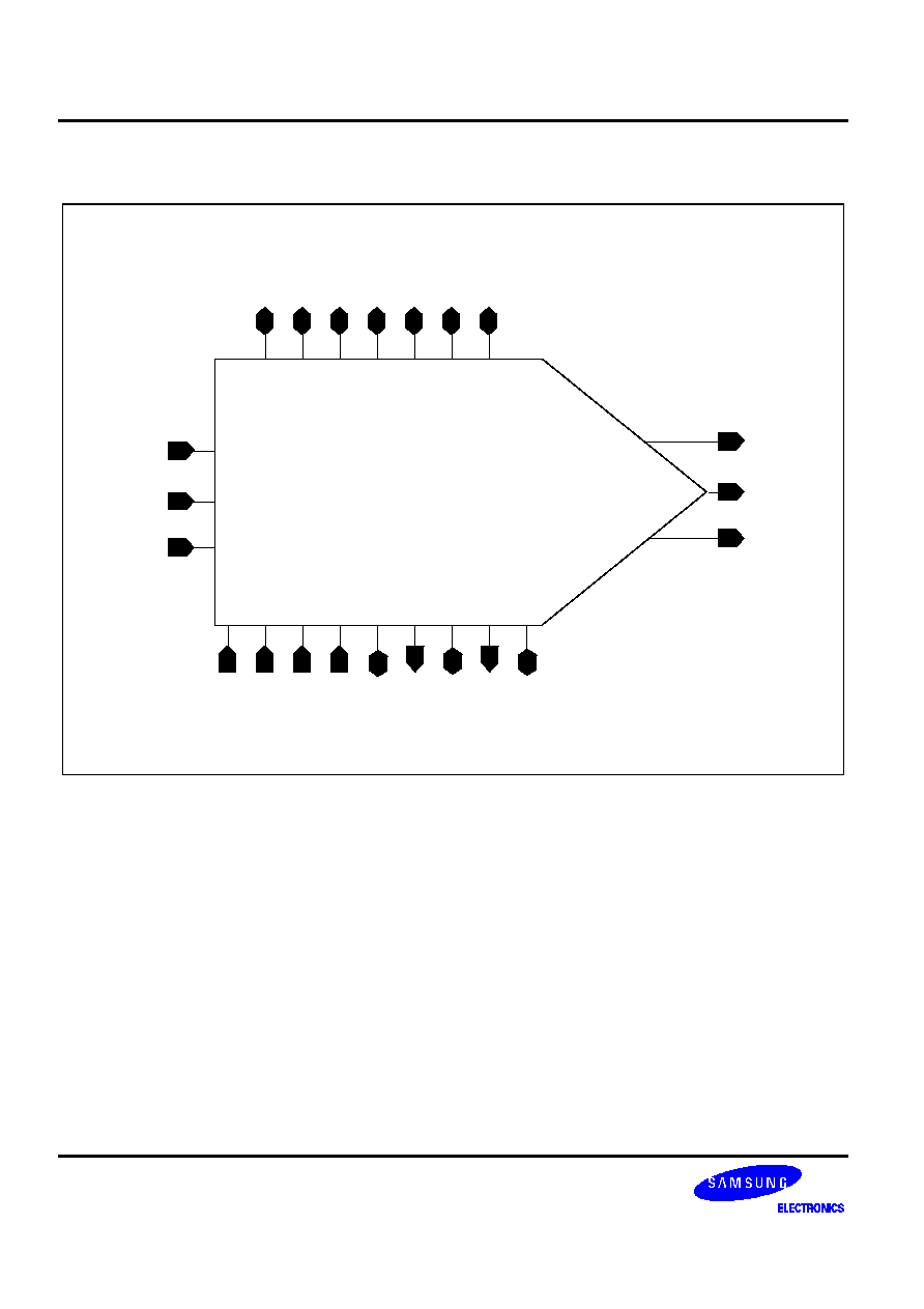
FUNCTIONAL BLOCK DIAGRAM
OPA M P
B GR
C M
SLEEP
( High Active)
VREFOUT
IRSET
SENSEZ
CCOMP
RA7~RA0
D A C 1
2'nd La tc h
1's t La tc h
D e c ode r1
GA7~GA0
D A C 2
2'nd La tc h
D e c ode r1
BA7~BA0
D A C 3
2'nd La tc h
D e c ode r1
CLK
BLANKEN
SETUP
I75uA
S E N S E
1 's t La tc h
1 's t La tc h
IOR
IOG
IOB

0.35
µ
µ
µ
µ
m 8-BIT 250MSPS DAC
BW2010D
3
CORE PIN DESCRIPTION
Name
I/O Type
I/O Pad
Pin Description
IOR,IOG,IOB
AO
poa_bb_50option
Analog DAC output (Red,Green,Blue)
RA0:RA7
DI
picc_bb
Video signal RED Digital input
GA0:GA7
DI
picc_bb
Video signal GREEN Digital input
BA0:BA7
DI
picc_bb
Video signal BLUE Digital input
CLK
DI
picc_bb
Clock
SLEEP
DI
picc_bb
Power down mode (hign active)
VREFOUT
AB
poa_bb_50option
Reference voltage input & monitoring
CCOMP
AB
poa_bb_50option
External capacitance connection
I75uA
AO
poa_bb
RAM drive 150 [uA] (for RAMDAC)
SENSEZ
AO
poar50_bb
DAC output sensing (for RAMDAC)
IRSET
AB
poa_bb_50option
external resistor connection
VSETUP
DI
picc_bb
Blank enable pin
BLANKEN
DI
picc_bb
7.5 IRE level enable
VDDA1
AP
vdda
Analog Power
VDDA2
AP
vdda
Analog Power
VDDD
DP
vddd
Digital Power
VSSA1
AG
vssa
Analog Ground
VSSA2
AG
vssa
Analog Ground
VSSD
DG
vssd
Digital Ground
VBBA
AG
vbba
Analog Ground
I/O Type Abbr.
-- AI: Analog Input
-- DI: Digital Input
-- AO: Analog Output
-- DO: Digital Output
-- AB: Analog Bidirectional
-- DB: Digital Bidirectional
-- AP: Analog Power
-- DP: Digital Power
-- AG: Analog Ground
-- DG: Digital Ground
BW2010D
0.35
µ
µ
µ
µ
m 8-BIT 250MSPS DAC
4
CORE CONFIGURATION
VSETUP SLEEP
CLK
CCOMPSENSEZ
IRSET
I75UA VREFOUT
RA[7:0]
GA[7:0]
BA[7:0]
VDDA1
VDDA2 VSSA2
VSSA1
VDDD
VSSD
VBBA
IOR
IOG
IOB
bw2010d
BLANKEN

0.35
µ
µ
µ
µ
m 8-BIT 250MSPS DAC
BW2010D
5
FUNCTIONAL DESCRIPTION
This Core is 8bit 250MSPS digital to analog data converter and uses segment architecture for 4bits of MSB sides
and binary-weighted architecture for 4bits of LSB side. It contains of First Latch Block, Decoder Block ,Second
Latch Block, OPA Block, BGR Block, Switch Buffer Block, Sleep Block for power down, CM(current mirror) Block
and Analog Switch Block. This core uses reference current to decide the 1LSB current size by dividing the
reference current by 122times. So the reference current must be constant and the switch's physical real size can
be constant by using OPA block with high DC gain. The most significant block of this core is analog switch block
and it must maintain the uniformity at each switch, so Layout designer must care about the matching
characteristics on analog switch and CM block. And more than 80% of supply current is dissipated at Analog
Switch Block and OPA Block. And it uses samsung(SEC) standard cell as all digital cell of latch, decoder and
buffer. And to adjust full current output, you must decide the "Rset" resistor value(connected to IRSET pin) and
"Vbias" voltage value(connected to VREFOUT pin). Its voltage output can be obtained by connecting
RL1(connected to IOR,IOG,IOB pin) .
Error: Linearity error is defined as the maximum deviation of the actual analog output from the ideal output,
determined by a straight line drawn from zero to full scale.
Monotonicity: A D/A converter is monotonic if the output either increases or remains constants as the digital
input increases.
Offset Error: The deviation of the output current from the ideal of zero is called offset error. For IO, 0mV output
expected when the inputs are all 0s.
Gain Errors: The difference between the actual andideal output span. The actual span is determined by the output
when all inputs are set to 1s minus the output when all inputs are set to 0s.
Output Compliance Range: The range of allowable voltage at the output of a current-output DAC. Operation
beyond the maximum compliance limits may cause either output stage saturation or breakdown resulting in
nonlinear performance.
Settling Time: The time required for the output to reach and remain within a specified error band about its final
value, measured from the start of the output transition
Glitch Impulse: Asymmetrical switching times in a DAC give rise to undesired output transients that are quantified
by a glitch impulse. It is specified as the net area of the glitch in pV-s

BW2010D
0.35
µ
µ
µ
µ
m 8-BIT 250MSPS DAC
6
ABSOLUTE MAXIMUM RATINGS
Characteristics
Symbol
Values
Unit
Supply Voltage
VDDA1
VDDA2
VDDA
-0.3 TO 7.0
V
Voltage on any Digital Voltage
Vin
VSSA-0.3 to VDDA+0.3
V
Storage Temperature Range
Tstg
-45 to 150
∫C
NOTES:
1. It is strongly recommended that to avoid power latch-up all the supply Pins(VDDA1,VDDA2,VSSA1,VSSA2,VDDA,VSSA)
be driven from the same source.
2. Absolute Maximum Rating values applied individually while all other parameters are within specified operating conditions.
Function operation under any of these conditions is not implied.
3. Applied voltage must be current limited to specified range.
4. Absolute Maximum Ratings are value beyond which the device may be damaged permanently. Normal operation is not
guaranteed.
RECOMMENDED OPERATING CONDITIONS
Characteristics
Symbol
Min
Typ
Max
Unit
Operating Supply Voltage
VDDA
3.15
3.3
3.45
V
Digital input Voltage HIGH
LOW
Vih
Vil
0.7VDDA
-
-
-
-
0.3VDDA
V
Operating Temperature Range
Topr
0
25
70
∫C

0.35
µ
µ
µ
µ
m 8-BIT 250MSPS DAC
BW2010D
7
DC ELECTRICAL CHARACTERISTICS
Characteristics
Symbol
Min
Typ
Max
Unit
Resolution
-
-
8
-
Bits
Differential Linearity Error
DLE
-1
0.1
+1
LSB
Integral Linearity Error
ILE
-1
0.2
+1
LSB
Monotonicity
-
-
Guaranteed
-
-
White to Black Pedestral Voltage
-
0.55
0.6
0.65
V
Maximum Output Compliance
Voc
-0.3
-
+1.3
V
Exteranl Reference Voltage (option)
-
1.2
1.235
1.27
V
Internal BGR Reference Voltage
-
1.15
1.235
1.25
V
Power Supply Current
Is
60
66
67
mA
NOTES:
1.
White to Black Pedestal Voltage can be changed by using external RSET resistor
2.
Converter Specifications (unless otherwise specified)
VDDA=3.3V VSSA=GND
Ta=25∫C RL=37.5Ohm , VREFOUT=1.235V
AC ELECTRICAL CHARACTERISTICS
Characteristics
Symbol
Min
Typ
Max
Unit
Conversion Speed
Fop
-
250
300
MHz
Analog Output Delay
Td
-
1
-
ns
Analog Output Rise Time
Tr
-
0.5
1
ns
Analog Output Fall Time
Tf
-
0.5
1
ns
Analog Output Settling Time
Ts
-
40
55
ns
Glitch Impulse
GI
-
50
70
pVsec
Feedthrough
fdth
17
18
-
dB
Setup Time
Ts
-
0.3
0.5
nsec
Hold Time
Th
-
0.3
0.5
nsec
Output Compliance
Voc
-0.3
-
1.3
V
THD(Total Harmonic Distortion)
THD
-
0.125
-
%
SNDR( Fin=6MHz , Fck=300MHz)
SNDR
44
47
-
dB
NOTES:
1.
The above parameters are guaranteed over the full temperature range.
2.
Clock and data feed-through is a function of the amount of overshoot and undershoot on the digital inputs .Settling time
does not include clock and data feed-through . Glitch impulse include clock and data feed-through.
3.
Setup and Hold Time are simulation values, not a test result

BW2010D
0.35
µ
µ
µ
µ
m 8-BIT 250MSPS DAC
8
TIMING DIAGRAM (FOR ONE CHANNEL)
D[7:0]
IO
Ts
50%
Tset
Th
Td
0.1%
Half clock pipeline delay
CLK
NOTES:
1.
Output delay measured from the 50% point of the rising edge of CLK to the full scale transition
2.
Settling time measured from the 50% point of full scale transition to the output remaining within ±1, ±2LSB.
3.
Output rise/fall time measured between the 10% and 90% points of full scale transition.
4.
Power Down On Time : 5.5us , Power Down Off Time : 5.5ms

0.35
µ
µ
µ
µ
m 8-BIT 250MSPS DAC
BW2010D
9
TIMING DIAGRAM (FOR ONE CHANNEL)
100 IRE
BLACK LEVEL
BLANK LEVEL
WHITE LEVEL
7.5 IRE
0.714
0.54
0
7.5 IRE disable
7.5 IRE enable
mA
V
mA
V
R/G/B output
19.04
1.44
0
0.66
0
17.6
0
NOTE:
1. OUTPUT CONNECTED TO A DOUBLY TERMINATED 75
LOAD
2. Vref = 0.7V, Rset=1.27 K
IRE FUNCTION (FOR EACH CHANNEL)
Binary Input
Dac Output Current(Ma)
RL = 37.5 Ohm
Vsetup
Blanken
Data
Code
R,G,B Channel
0
0
000H
3FFH
0
1023
1.44
19.04
1
0
000H
3FFH
0
1023
1.44
19.04
0
1
000H
3FFH
0
1023
1.44
19.04
1
1
000H
3FFH
0
1023
0
17.6

BW2010D
0.35
µ
µ
µ
µ
m 8-BIT 250MSPS DAC
10
CORE EVALUATION GUIDE
SELECT
bw2010d
MAIN
PATH
RA<7:0>
16
8
8
8
8
8
CCOMP
Cc
BLANKEN
VSETUP
SENSEZ
I75uA
IRSET
R1
SLEEP(GND)
VREFOUT
CLK
1.235V
selection
option
VDDA VSSA
3.3V
Cc
Ct
+
VDDA1
VSSA1
Cc
Ct
+
3.3V
VDDA2 VSSA2
3.3V
Cc
Ct
+
GA<7:0>
BA<7:0>
IOR
R2
R2
R2
VBBA
IOG
IOB
MUX
Bi-drectional PAD
DAC function Measuring&Digitla input forcing
Location
Description
Cc
0.1uF
R1
147 Ohm
R2
37.5 Ohm
Ct
10uF
Cc
0.1uF

0.35
µ
µ
µ
µ
m 8-BIT 250MSPS DAC
BW2010D
11
1.Testability
Whether you use MUX or the internal logic for testability, it is required to be able to select the values of digital
inputs ,TEST PATH block 16pins. See above figure. Only if it is, you can check the main function (Linearity) and
output (IOR,IOG,IOB), VREFOUT ,IRSET and CCOMP pins are reserved for external use.
2. Analysis
The voltage applied to VREFOUT is measured at IRSET node . And the voltage value is proportioned to the
reference current value of resistor which is connected to IRSET node. So you can estimate the full scale current
value by measuring the voltage, and check the DC characteristics of the OPAMP. For reference, as VREFOUT
applied to CCOMP node is given at IRSET node, the current flowing through IRSET is given as VREFOUT/RSET.
The voltage is scaled factor of 1/122 for VIDEO. The full scale current is given as the decimal value equivalent to
the digital code.
* Resolution
If you want to change the resolution, use as many appear bits as you want and connect the rest lower bits to the
ground as above diagram which is 8bit application.
* Output Range Alteration
In order to change the output swing, use following equation.
Vout = {VREFOUT/(RSETx122)}xDAC_CODExRio

BW2010D
0.35
µ
µ
µ
µ
m 8-BIT 250MSPS DAC
12
PHANTOM CELL INFORMATION
-- Pins of the core can be assigned externally (Package pins) or internally (internal ports) depending on design
methods. The term "External" implies that the pins should be assigned externally like power pins. The term
"External/internal" implies that the applications of these pins depend on the user.
BW2010D
8bit tripe 250MSPS DAC
VB
B
A
VB
B
A
VS
E
T
U
P
B
L
A
NKE
N
VDDA1
VSSA1
VDDA2
IRSET
VSSA2
VDDA2
RA[7]
VS
S
D
V
DDD
CL
K
RA[6]
RA[5]
RA[4]
RA[3]
RA[2]
RA[1]
RA[0]
GA[7]
GA[6]
GA[5]
GA[4]
GA[3]
GA[2]
GA[1]
GA[0]
BA[7]
BA[6]
BA[5]
BA[4]
BA[3]
BA[2]
BA[1]
BA[0]
IOR
VDDA2
IOG
VREFOUT
CCOMP
IOB
VSSA2
SL
E
E
P
VS
S
D
V
DDD
VB
B
A
VB
B
A

0.35
µ
µ
µ
µ
m 8-BIT 250MSPS DAC
BW2010D
13
PHANTOM CELL INFORMATION (Continued)
Pin Name
Pin Usage
Pin Layout Guide
VDDD
External
- Maintain the large width of lines as far as the pads.
- place the port positions to minimize the length of power lines.
- Do not merge the analog powers with another power from other blocks.
- Use good power and ground source on board.
VSSD
External
VBBA
External
VDDA1
External
VSSA1
External
VDDA2
External
VSSA2
External
CCOMP
External/Internal - Do not overlap with digtal lines.
- Maintain the shortest path to pads.
VREFOUT
External/Internal
IREF
External/Internal - Separate from all other analog signals
IOR
External/Internal - Maintain the larger width and the shorter length as far as the pads.
- Separate from all other digital lines.
IOG
External/Internal
IOB
External/Internal
SLEEP
External/Internal - Separated from the analog clean signals if possible.
- Do not exceed the length by 1,000um.
BLANKEN
External/Internal
VSETUP
External/Internal
RA[7:0]
External/Internal
GA[7:0]
External/Internal
BA[7:0]
External/Internal

BW2010D
0.35
µ
µ
µ
µ
m 8-BIT 250MSPS DAC
14
PACKAGE CONFIGURATION
NC
IRSET
NC
48
VDDA2
SENSEZ
VBBA
VSSA
I75uA
CLK
SLEEP
47
46
45
44
43
42
41
40
39
38
37
36
35
34
33
32
31
30
29
28
27
26
25
VDDA
VDDA1
VSSA2
R=37.5Ohm
VDDA2
VSSA2
IOR
IOG
IOB
BLANKE N
NC
CCOMP
VREFOUT
VSSA1
BA4
BA5
BA6
BA7
GA0
11
12
13
14
15
16
17
18
19
20
BA0
BA1
BA2
BA3
21
22
23
24
GA1
GA2
GA3
GA4
GA5
GA6
GA7
RA0
RA1
RA2
RA3
RA4
RA5
RA6
RA7
1
2
3
4
5
6
7
8
9
10
250 MHz
+1.235V
R=147 Ohm
digital
input
data
Cc
C1
C2
normal 0V operation
+3.3V
C1
C2
+3.3V
C1
C2
+3.3V
C1
C2
0V
3.3V
0V
3.3V
R=37.5Ohm
R=37.5Ohm
0V
3.3V
VSE TUP
Location
Description
Cc
0.1uF TANTALUM CAPACITOR
C1
10uF CAPACITOR
C2
0.1uF CERAMIC CAPACITOR
Rio
37.5 ohm 1% RESISTOR
RSET
147 ohm 1% METAL FILM RESISTOR
NOTES:
1.
Analog and digital supplies should be separated and de-coupled.
2. Supplies are not connected internally
3.
All ground pins must be connected. One ground plane is preferred although it depends on the application

0.35
µ
µ
µ
µ
m 8-BIT 250MSPS DAC
BW2010D
15
PACKAGE PIN DESCRIPTION
Pin Name
No
I/O Type
Description
BA<0:7>
1~8
DI
Video signal BLUE Digital input
GA<0:7>
9~16
DI
Video signal GREEN Digital input
RA<0:7>
17~24
DI
Video signal RED Digital input
VREFOUT
43
AI
Reference voltage input & monitoring
IRSET
32
AI
external resistor connection
SLEEP
45
DI
Power down mode (hign active)
BLANKEN
26
DI
Blank enable pin
VSETUP
27
DI
7.5 IRE level enable
CLK
46
DI
Clock
I75uA
36
AO
RAM drive (150 [uA] )
CCOMP
38
AI
External capacitance connection
SENSEZ
34
AO
DAC output sensing
IOR
35
AO
Analog Voltage Output
IOG
37
AO
Analog Voltage Output
IOB
39
AO
Analog Voltage Output
VDDA
48
DP
Digital Power
VSSA
47
DG
Digital Ground
VBBA
25
AG
Bulk Bias Ground
VDDA1
30
AP
Analog Power
VDDA2
33,40
AP
Analog Power
VSSA1
29
AG
Analog Ground
VSSA2
31,42
AG
Analog Ground
NOTE: I/O TYPE PP and PG denote PAD Power and PAD Ground respectively.

BW2010D
0.35
µ
µ
µ
µ
m 8-BIT 250MSPS DAC
16
FEEDBACK REQUEST
We appreciate your interest in out products.
If you have further questions, please specify in the attached form.
Thank you very much.
DC / AC ELECTRICAL CHARACTERISTIC
Characteristics
Min
Typ
Max
Unit
Remarks
Supply Voltage
V
Power dissipation
mW
Resolution
Bits
Analog Output Voltage
V
Operating Temperature
∞
C
Output Load Capacitor
pF
Output Load Resistor
k
Integral Non-Linearity Error
LSB
Differential Non-Linearity Error
LSB
Maximum Conversion Rate
MHz
VOLTAGE OUTPUT DAC
Reference Voltage TOP
BOTTOM
V
Analog Output Voltage Range
V
Digital Input Format
Binary Code or 2's Complement Code
CURRENT OUTPUT DAC
Analog Output Maximum Current
mA
Analog Output Maximum Signal Frequency
kHz
Reference Voltage
V
External Resistor for Current Setting(RSET)
Pipeline Delay
sec
-- Do you want to Power down mode?
-- Do you want to Internal Reference Voltage(BGR)?
-- Which do you want to serial input data type or parallel input type?

0.35
µ
µ
µ
µ
m 8-BIT 250MSPS DAC
BW2010D
17
VERSION LIST
Version
Date
Modified Items
Comments
Ver 1..0
98.05.01
Original version published
Ver 1.4
99.12.13
1. Test configuration correction 2. Font correction
Ver 1.5
20.02.23
1. font correction 2. layout guide correction
Ver 1.6
02.0420
Add item (Phantom cell guide)

BW2010D
0.35
µ
µ
µ
µ
m 8-BIT 250MSPS DAC
18
NOTES