
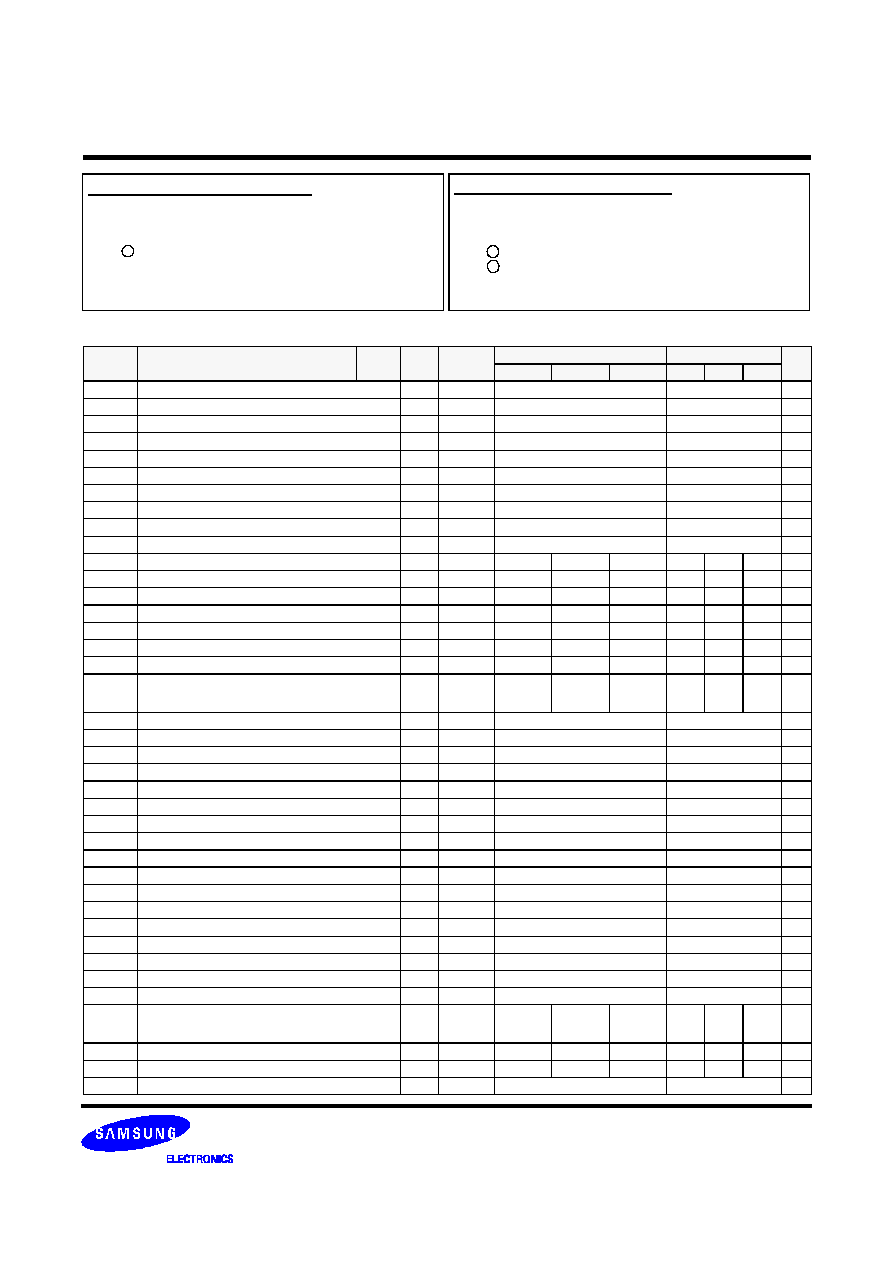
SERIAL PRESENCE DETECT
MR16R0824(6/8/C/G)BN1
- 1 -
RAMBUS MODULE
Version 1.1 Oct. 2000
Change History
Version 1.1 (Oct.
00)
Based on the Samsung 128M RDRAM (A-die) SPD Specification 1.02 version.
based on 128M RDRAM
(B-die, 32s banks)
RIMM SPD Specification
Version 1.1
October 2000
SERIAL PRESENCE DETECT
MR16R0824(6/8/C/G)BN1
- 2 -
RAMBUS MODULE
Version 1.1 Oct. 2000
� Contents ;
Byte #
(Dec)
Described Function
Option
Field
Width
Units
Supported Function
Hex Value
Note
K8
K7
G6
K8
K7
G6
0
SPD Revision Level
8
LUT
SPD Revision 1.0
02h
1
1
Total Number of Bytes in the SPD
8
LUT
256 Bytes
08h
1
2
Device Type
8
LUT
Direct RDRAM
01h
1
3
Module Type
8
LUT
RIMM Module
01h
1
4
Row Address Bits[3:0], Column Address Bits[3:0]
4,4
bits
9 bits, 6 bits
96h
5
Bank Address Bits and Type
8
LUT
32s banks
C5h
1
6
Refresh Bank Bits
3
bits
32 Refresh Bank Sets
05h
7
Refresh Period(=t
REF
)
8
ms
32ms
20h
8
Protocol Version
8
LUT
Protocol Version 1
02h
1
9
Misc. Device Configuration Field
8
n/a
DQS=1.5
,
no -LP, S28, S3
05h
3
10
Minimum Precharge to RAS time(=t
RP-R,Min
)
5
1/f
RAS
8cycles
8cycles
8cycles
08h
08h
08h
11
Minimum RAS to Precharge time(=t
RAS-R
,
Min
)
6
1/f
RAS
20cycles
20cycles
20cycles
14h
14h
14h
12
Minimum RAS to CAS time(=t
RCD-R,Min
)
5
1/f
RAS
10cycles
8cycles
8cycles
0Ah
08h
08h
13
Minimum RAS to RAS time(=t
RR-R,Min
)
5
1/f
RAS
8cycles
8cycles
8cycles
08h
08h
08h
14
Minimum Precharge to Precharge time(=t
PP-R,Min
)
5
1/f
RAS
8cycles
8cycles
8cycles
08h
08h
08h
15
Min t
CYCLE
for Range A
8
128ps
2.50ns
2.80ns
3.33ns
13h
15h
1Ah
16
Max t
CYCLE
for Range A
8
128ps
3.83ns
3.83ns
3.83ns
1Eh
1Eh
1Eh
17
t
CDLY
Range for Range A
8
t
CYCLE
5t
CYCLE
~ 9t
CYCLE
5t
CYCLE
~ 9t
CYCLE
5t
CYCLE
~ 9t
CYCLE
59h
59h
59h
18
t
CLS
and t
CAS
Range for Range A
8
t
CYCLE
2t
CYCLE
for t
CLS
& t
CAS
AAh
19
Min t
CYCLE
for Range B
8
128ps
RFU
00h
2
20
Max t
CYCLE
for Range B
8
128ps
RFU
00h
2
21
t
CDLY
Range for Range B
8
t
CYCLE
RFU
00h
2
22
t
CLS
and t
CAS
Range for Range B
8
t
CYCLE
RFU
00h
2
23
Min t
CYCLE
for Range C
8
128ps
RFU
00h
2
24
Max t
CYCLE
for Range C
8
128ps
RFU
00h
2
25
t
CDLY
Range for Range C
8
t
CYCLE
RFU
00h
2
26
t
CLS
and t
CAS
Range for Range C
8
t
CYCLE
RFU
00h
2
27
Min t
CYCLE
for Range D
8
128ps
RFU
00h
2
28
Max t
CYCLE
for Range D
8
128ps
RFU
00h
2
29
t
CDLY
Range for Range D
8
t
CYCLE
RFU
00h
2
30
t
CLS
and t
CAS
Range for Range D
8
t
CYCLE
RFU
00h
2
31
Power Down Exit Max.time, Phase A(=t
PDNXA,Max
)
8
us
4us
04h
32
Power Down Exit Max.time, Phase B(=t
PDNXB,Max
)
8
64t
CYCLE
9000t
CYCLE
8Dh
33
Nap Exit Max.time, Phase A(=t
NAPXA,Max
)
8
ns
50ns
32h
34
Nap Exit Max.time, Phase B(=t
NAPXB,Max
)
8
ns
40ns
28h
35
f
IMIN
[11:8]
f
IMAX
[11:8]
4
4
MHz
261MHz
400MHz
261MHz
357MHz
261MHz
300MHz
11h
11h
11h
36
f
IMIN
[7:0]
8
MHz
261MHz
261MHz
261MHz
05h
05h
05h
37
f
IMAX
[7:0]
8
MHz
400MHz
357MHz
300MHz
90h
65h
2Ch
38
ODF mapping
-
-
-
00h
1
MR16R082C(G)BN1-CK8/CK7/CG6
� Feature : Double Sided Module & 1,250 mil height
� Composition : 8Mx16 *12(16)pcs
� Used component type & part number
Normal Package (K4R271669B-NCK8/NCK7/NCG6)
Mirrored Package (K4R271669B-MCK8/MCK7/MCG6)
� # of banks in component :32s banks (Doubled with Split Banks)
� Refresh : 16K/32ms
MR16R0824(6/8)BN1-CK8/CK7/CG6
� Feature : Single Sided Module & 1,250 mil height
� Composition : 8Mx16 *4(6/8)pcs
� Used component type & part number
Normal Package (K4R271669B-NCK8/NCK7/NCG6)
� # of banks in component : 32s banks (Doubled with Split Banks)
� Refresh : 16K/32ms
1
2
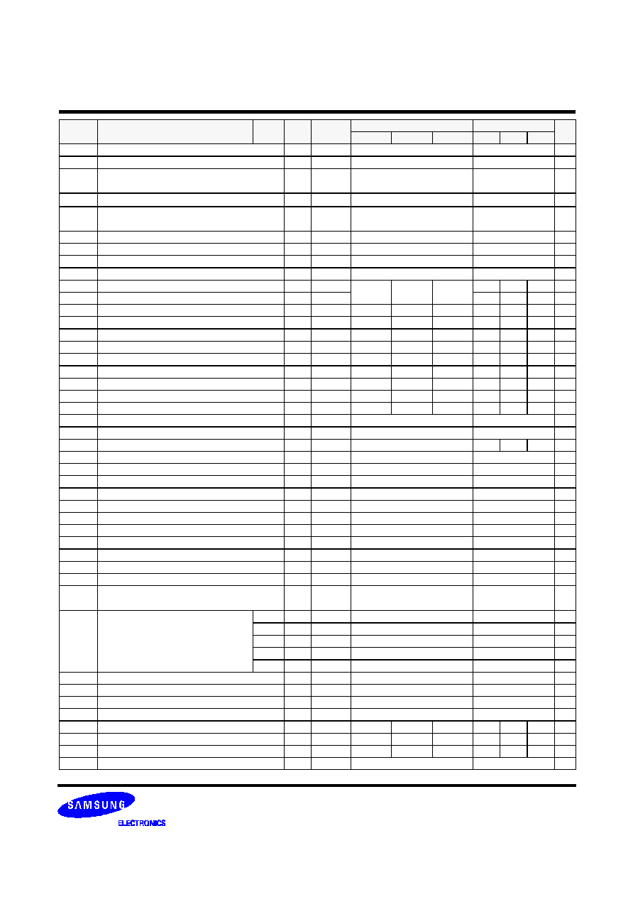
SERIAL PRESENCE DETECT
MR16R0824(6/8/C/G)BN1
- 3 -
RAMBUS MODULE
Version 1.1 Oct. 2000
39
Max. time between Current Control(=t
CCTRL,Max
)
8
ms
100ms
64h
40
Max. time between Temp. Calibration(=t
TEMP,Max
)
8
ms
100ms
64h
41
Min. time between Temp. Calibration Enable
and Command(=t
TCEN,Min
)
8
t
CYCLE
150t
CYCLE
96h
42
Maximum RAS to Precharge time(=t
RAS-R,Max
)
8
us
64us
40h
43
Maximum time that a Device can stay in Nap
Mode(=t
NLIMIT,Max
)
8
us
10us
0Ah
44
ACTREFPT[3:0], PCHREFPT[3:0]
4,4
t
CYCLE
6t
CYCLE,
6t
CYCLE
66h
45
CPCHREFPT_DC[3:0], RDREFPT_DC[3:0]
4,4
t
CYCLE
5t
CYCLE,
5t
CYCLE
55h
46
RETREFPT_DC[3:0], WRREFPT_DC[3:0]
4,4
t
CYCLE
5t
CYCLE,
13t
CYCLE
5Dh
47~49
Reserved
-
-
-
00h
50
f
RAS
[11:8]
4
MHz
400MHz
357MHz
300MHz
01h
01h
01h
51
f
RAS
[7:0]
8
MHz
90h
65h
2Ch
52
PMAX,HI, PMAX,LO, Tj
1,1,6
�
C
0,0,100
�
C 0,0,100
�
C 0,0,100
�
C
24h
24h
24h
53
HeatSpreader, thermal sensor, Tplate
1,1,6
�
C
1,0, 92
�
C
1,0,92
�
C
1,0,92
�
C
9Ch
9Ch
9Ch
54
PSTBY,HI
8
1mA
105mA
100mA
90mA
69h
64h
5Ah
55
PACTI,HI
8
2mA
165mA
155mA
140mA
52h
4Dh
46h
56
PACTRW,HI
8
8mA
575mA
525mA
455mA
47h
41h
38h
57
PSTBY,LO
8
1mA
80mA
80mA
80mA
50h
50h
50h
58
PACTI,LO
8
2mA
135mA
135mA
135mA
43h
43h
43h
59
PACTRW,LO
8
8mA
410mA
410mA
410mA
33h
33h
33h
60
PNAP
8
128uA
4.0mA
4.0mA
4.0mA
1Fh
1Fh
1Fh
61
PRESA (Reserved for a future thermal parameter)
-
-
-
00h
62
PRESB (Reserved for a future thermal parameter)
-
-
-
00h
63
Checksum for bytes 0 ~ 62
8
n/a
-
86h
20h
99h
3
64
Module Manufacturer ID Code
8
n/a
Samsung
CEh
3
65~71
...... Module Manufacturer ID Code
56
n/a
Samsung
00h
3
72
Module Manufacturer Location
8
n/a
Onyang Korea
01h
3
73
Module Part Number(Memory module)
8
n/a
M
4Dh
3
74
Module Part Number(Module Configuration)
8
n/a
R
52h
3
75
Module Part Number(Data Bits)
8
n/a
1
31h
3
76
...... Module Part Number(Data Bits)
8
n/a
6
36h
3
77
Module Part Number(Feature)
8
n/a
R
52h
3
78
Module Part Number(Module Density)
8
n/a
Blank
20h
3
79
Module Part Number(Module Density)
8
n/a
0
30h
3
80
...... Module Part Number(Module Density)
8
n/a
8
38h
3
81
Module Part Number
(Refresh, # of banks in comp. & interface)
8
n/a
2
32h
3
82
Module Part Number(# of component )
4d
8
n/a
4
34h
3
6d
8
n/a
6
36h
3
8d
8
n/a
8
38h
3
12d
8
n/a
C
43h
3
16d
8
n/a
G
47h
3
83
Module Part Number(Component Revision)
8
n/a
B
42h
3
84
Module Part Number(Package Type)
8
n/a
N
4Eh
3
85
Module Part Number(PCB Revision)
8
n/a
1
31h
3
86
Module Part Number(Hyphen)
8
n/a
- (Hyphen)
2Dh
3
87
Module Part Number(Power)
8
n/a
C
C
C
43h
43h
43h
3
88
Module Part Number(t
RAC
& Speed)
8
n/a
K
K
G
4Bh
4Bh
47h
3
89
Module Part Number(t
RAC
& Speed)
8
n/a
8
7
6
38h
37h
36h
3
90
Module Part Number(RFU)
8
n/a
-
00h
3
Byte #
(Dec)
Described Function
Option
Field
Width
Units
Supported Function
Hex Value
Note
K8
K7
G6
K8
K7
G6

SERIAL PRESENCE DETECT
MR16R0824(6/8/C/G)BN1
- 4 -
RAMBUS MODULE
Version 1.1 Oct. 2000
<Notes>
1. Please refer to Look-Up Table (LUT) in the Direct Rambus
TM
SPD specification 1.0
2. It is reserved to future use (RFU).
3. Unit is not available ( n/a).
4. These bytes are programmed by code of Date Week & Date Year with binary format.
5. These bytes are programmed by Samsung's own Module Assembly Serial # system. All modules may have unique serial #.
91
Module Manufacturer Revision Code (PCB)
8
n/a
1
31h
3
92
...... Component Manufacturer Revision Code
8
n/a
B (B die)
42h
3
93
Module Manufacturing Year
8
n/a
-
-
3, 4
94
Module Manufacturing Week
8
n/a
-
-
3, 4
95~98
Module Serial Number
32
n/a
-
-
3, 5
99
Number of Devices on Module
4d
6
devices
4
04h
6d
6
devices
6
06h
8d
6
devices
8
08h
12d
6
devices
12
0Ch
16d
6
devices
16
10h
100
Module Data Width
8
bits
16bits
10h
101
Devices Enables
4d
8
bits
All 4 devices are enabled
0Fh
6d
8
bits
All 6 devices are enabled
3Fh
8d
8
bits
All 8 devices are enabled
FFh
12d
8
bits
All 12 devices are enabled
FFh
16d
8
bits
All 16 devices are enabled
FFh
102
...... Devices Enables
4d
8
bits
All 4 devices are enabled
00h
6d
8
bits
All 6 devices are enabled
00h
8d
8
bits
All 8 devices are enabled
00h
12d
8
bits
All 12 devices are enabled
0Fh
16d
8
bits
All 16 devices are enabled
FFh
103~104 ...... Devices Enables
16
bits
-
00h
105
Module Vdd[3:0],
Module Voltage Interface Level[3:0]
4,4
LUT
2.5V, 1.8V Vterm
10h
1
106
Module Vdd Tolerance
8
LUT
5% DC, 2% AC
52h
1
107~113 Reserved
56
-
-
00h
114
CDLY0/1 for tCDLY=3
8
t
CYCLE
-
00h
115
CDLY0/1 for tCDLY=4
8
t
CYCLE
-
00h
116
CDLY0/1 for tCDLY=5
8
t
CYCLE
3 / 0
30h
117
CDLY0/1 for tCDLY=6
8
t
CYCLE
3 / 1
31h
118
CDLY0/1 for tCDLY=7
8
t
CYCLE
3 / 2
32h
119
CDLY0/1 for tCDLY=8
8
t
CYCLE
4 / 2
42h
120
CDLY0/1 for tCDLY=9
8
t
CYCLE
5 / 2
52h
121
CDLY0/1 for tCDLY=10
8
t
CYCLE
-
00h
122
CDLY0/1 for tCDLY=11
8
t
CYCLE
-
00h
123
CDLY0/1 for tCDLY=12
8
t
CYCLE
-
00h
124
CDLY0/1 for tCDLY=13
8
t
CYCLE
-
00h
125
CDLY0/1 for tCDLY=14
8
t
CYCLE
-
00h
126
CDLY0/1 for tCDLY=15
8
t
CYCLE
-
00h
127
Checksum for Bytes 99 ~ 126
4d
8
n/a
-
ACh
3
6d
8
n/a
-
DEh
8d
8
n/a
-
A0h
12d
8
n/a
-
B3h
16d
8
n/a
-
A7h
3
128 +
Open for Customer Use
-
-
-
Undefined
Byte #
(Dec)
Described Function
Option
Field
Width
Units
Supported Function
Hex Value
Note
K8
K7
G6
K8
K7
G6