Page 1
MR18R162WDG0
Version 1.0 July. 2002
Overview
The RIMM
TM
module is a general purpose high- perfor-
mance memory module suitable for use in a broad range of
applications computer memory, personal computers, work-
stations, and other applications where high bandwidth and
low latency are required.
The RIMM module consists of 288Mb Direct RDRAM
devices. These are extremely high-speed CMOS DRAMs
organized as 16M words by 18 bits. The use of Rambus
Signaling Level (RSL) technology permits 800 MHz
transfer rates while using conventional system and board
design technologies. RDRAM devices are capable of
sustained data transfers at 1.25 ns per two bytes (10ns per 16
bytes).
The RDRAM architecture enables the highest sustained
bandwidth for multiple, simultaneous, randomly addressed,
memory transactions. The separate control and data buses
with independent row and column control yield over 95%
bus efficiency.
Features
High speed 800MHz RDRAM storage
184 edge connector pads with 1mm pad spacing
Module PCB size : 133.35mm x 69.85mm x 1.27mm
(5.25
"
x 2.75
"
x 0.05
"
)
Each RDRAM has 32 banks, for a total of 1024 banks on
1152MB module
Gold plated edge connector pad contacts
Serial Presence Detect(SPD) support
Operates from a 2.5 volt supply (� 5%)
Powerdown self refresh modes
Separate Row and Column buses for higher efficiency
WBGA lead free Package (92 balls)
Key Timing Parameters/Part Numbers
The following table lists the frequency and latency bins
available for RIMM modules.
Table 1: Part Number by Freq. & Latency
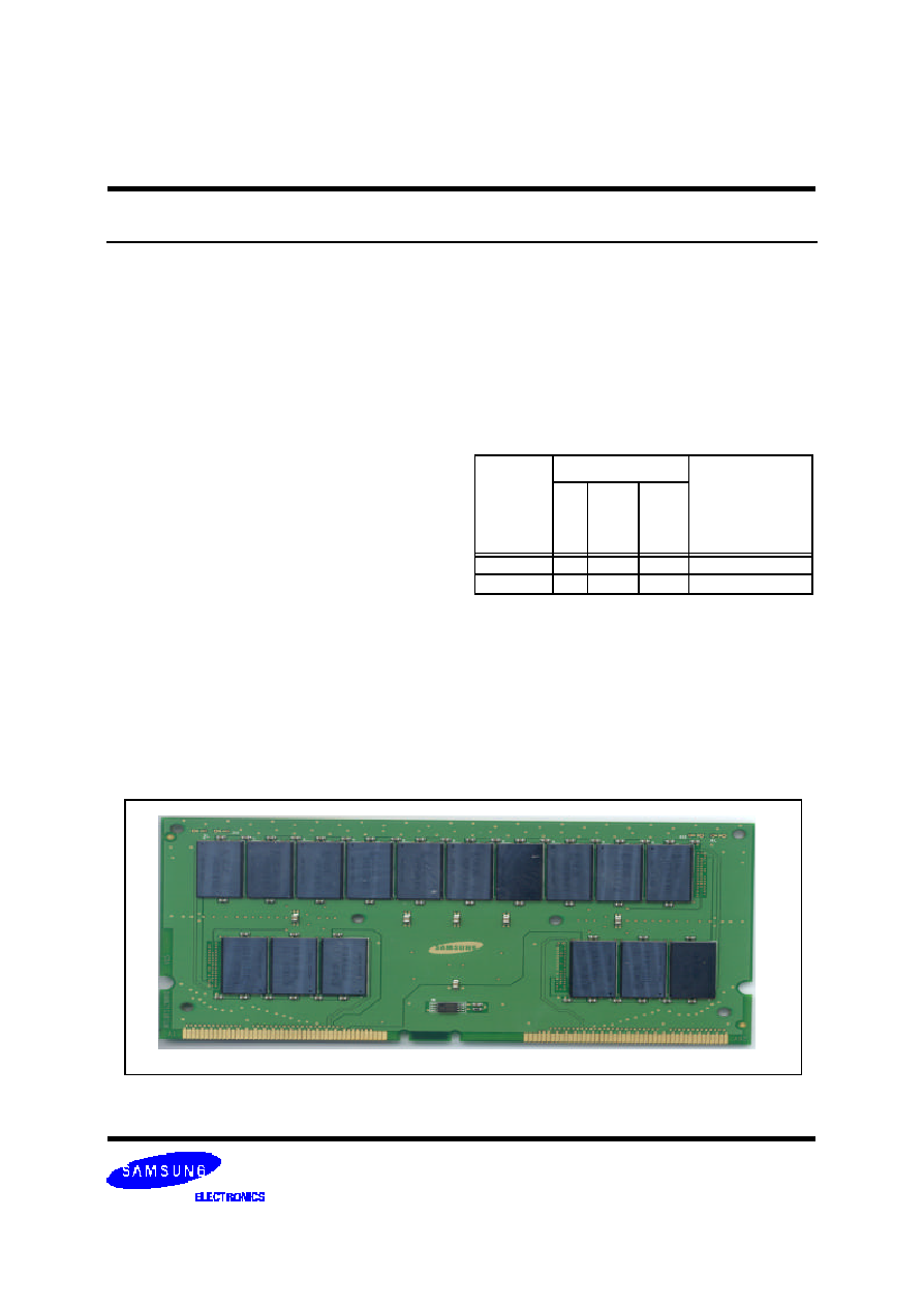
Form Factor
The RIMM modules are offered in 184-pad 1mm edge
connector pad pitch suitable for 184 contact RIMM connec-
tors. Figure 1 below, shows a thirty two device RIMM
module.
Organization
Speed
Part Number
Bin
I/O
Freq.
(MHz)
t
RAC
(Row
Access
Time) ns
512M x 18
-CK8
800
45
MR18R162WDG0-CK8
512M x 18
-CM8
800
40
MR18R162WDG0-CM8
(16Mx18)*32pcs RIMM
TM
Module based on 288Mb D-die, 32s banks,16K/32ms Ref, 2.5V
Figure 1: RIMM Module shown with heat spreader removed
Note: On double sided modules, RDRAMs are also installed on bottom side of PCB.
Page 3
MR18R162WDG0
Version 1.0 July. 2002
Table 3: Module Connector Pad Description
Signal
Pins
I/O
Type
Description
Gnd
A1, A3, A5, A7, A9, A11, A13, A15,
A17, A19, A21, A23, A25, A27, A29,
A31, A33, A39, A52, A60, A62, A64,
A66, A68, A70, A72, A74, A76, A78,
A80, A82, A84, A86, A88, A90, A92,
B1, B3, B5, B7, B9, B11, B13, B15,
B17, B19, B21, B23, B25, B27, B29,
B31, B33, B39, B52, B60, B62, B64,
B66, B68, B70, B72, B74, B76, B78,
B80, B82, B84, B86, B88, B90, B92
Ground reference for RDRAM core and interface. 72 PCB
connector pads.
LCFM
B10
I
RSL
Clock from master. Interface clock used for receiving RSL
signals from the Channel. Positive polarity.
LCFMN
B12
I
RSL
Clock from master. Interface clock used for receiving RSL
signals from the Channel. Negative polarity.
LCMD
B34
I
V
CMOS
Serial Command used to read from and write to the control
registers. Also used for power management.
LCOL4..
LCOL0
A20, B20, A22, B22, A24
I
RSL
Column bus. 5-bit bus containing control and address infor-
mation for column accesses.
LCTM
A14
I
RSL
Clock to master. Interface clock used for transmitting RSL
signals to the Channel. Positive polarity.
LCTMN
A12
I
RSL
Clock to master. Interface clock used for transmitting RSL
signals to the Channel. Negative polarity.
LDQA8..
LDQA0
A2, B2, A4, B4, A6, B6, A8, B8, A10
I/O
RSL
Data bus A. A 9-bit bus carrying a byte of read or write data
between the Channel and the RDRAM.
LDQB8..
LDQB0
B32, A32, B30, A30, B28, A28, B26,
A26, B24
I/O
RSL
Data bus B. A 9-bit bus carrying a byte of read or write data
between the Channel and the RDRAM.
LROW2..
LROW0
B16, A18, B18
I
RSL
Row bus. 3-bit bus containing control and address information
for row accesses.
LSCK
A34
I
V
CMOS
Serial Clock input. Clock source used to read from and write
to the RDRAM control registers.
NC
A16, B14, A44, B44, A45, B45, A46,
B46, A47, B47, A48, B48, A49, B49,
A77, B79
These pads are not connected. These 24 connector pads are
reserved for future use.
RCFM
B83
I
RSL
Clock from master. Interface clock used for receiving RSL
signals from the Channel. Positive polarity.
RCFMN
B81
I
RSL
Clock from master. Interface clock used for receiving RSL
signals from the Channel. Negative polarity.
RCMD
B59
I
V
CMOS
Serial Command Input. Pin used to read from and write to the
control registers. Also used for power management.
RCOL4..
RCOL0
A73, B73, A71, B71, A69
I
RSL
Column bus. 5-bit bus containing control and address infor-
mation for column accesses.
Page 4
MR18R162WDG0
Version 1.0 July. 2002
RCTM
A79
I
RSL
Clock to master. Interface clock used for transmitting RSL
signals to the Channel. Positive polarity.
RCTMN
A81
I
RSL
Clock to master. Interface clock used for transmitting RSL
signals to the Channel. Negative polarity.
RDQA8..
RDQA0
A91, B91, A89, B89, A87, B87, A85,
B85, A83
I/O
RSL
Data bus A. A 9-bit bus carrying a byte of read or write data
between the Channel and the RDRAM.
RDQB8..
RDQB0
B61, A61, B63, A63, B65, A65, B67,
A67, B69
I/O
RSL
Data bus B. A 9-bit bus carrying a byte of read or write data
between the Channel and the RDRAM.
RROW2..
RROW0
B77, A75, B75
I
RSL
Row bus. 3-bit bus containing control and address information
for row accesses.
RSCK
A59
I
V
CMOS
Serial Clock input. Clock source used to read from and write
to the RDRAM control registers.
SA0
B53
I
SV
DD
Serial Presence Detect Address 0.
SA1
B55
I
SV
DD
Serial Presence Detect Address 1.
SA2
B57
I
SV
DD
Serial Presence Detect Address 2.
SCL
A53
I
SV
DD
Serial Presence Detect Clock.
SDA
A55
I/O
SV
DD
Serial Presence Detect Data (Open Collector I/O).
SIN
B36
I/O
V
CMOS
Serial I/O for reading from and writing to the control registers.
Attaches to SIO0 of the first RDRAM on the module.
SOUT
A36
I/O
V
CMOS
Serial I/O for reading from and writing to the control registers.
Attaches to SIO1 of the last RDRAM on the module.
SV
DD
A56, B56
SPD Voltage. Used for signals SCL, SDA, SWE, SA0, SA1
and SA2.
SWP
A57
I
SV
DD
Serial Presence Detect Write Protect (active high). When low,
the SPD can be written as well as read.
V
CMOS
A35, B35, A37, B37
CMOS I/O Voltage. Used for signals CMD, SCK, SIN,
SOUT.
Vdd
A38, B38, A40, B40, A41, B41, A42,
B42, A43, B43, A50, B50, A54, B54,
A58, B58
Supply voltage for the RDRAM core and interface logic.
Vref
A51, B51
Logic threshold reference voltage for RSL signals.
Signal
Pins
I/O
Type
Description