6 4 C O M / 1 2 8 S E G G R A P H I C D R I V E R F O R D O T M A T RIX LCD
S6B0708
1
INTRODUCTION
S6B0708 is a single-chip LCD driver IC for liquid crystal dot-matrix graphic display systems. It incorporates 192
driver circuit for 64 common and 128 segment and 64 x 128-bit bit-map RAM. It is capable of interfacing with the
microprocessor, accepting 8-bit parallel display data directly from it, and storing data in an one chip display data
RAM. And it generates internal signals for using LCD driving independent of microprocessor clock.
FEATURES
∑
64-channel common & 128-channel segment driver for dot matrix LCD
∑
On-chip display data RAM: 64
◊
128 = 8192bits
∑
Display data is stored in display data RAM from MPU
- RAM bit data: ON(1), OFF(0)
∑
Internal timing generator circuit for dynamic display
∑
8-bit parallel bi-directional data bus
∑
Applicable LCD duty: 1/64
∑
Power supply voltages: Power supply voltage range: 4.5 - 5.5V (VDD)
∑
LCD driving voltage range: 8.0 - 17.0V (VLCD = VDD-VEE)
∑
Wide operating temperature range: Ta = -30
∞
C - 85
∞
C
∑
High voltage CMOS process
∑
Gold bumped chip available

S6B0708 6 4 C O M / 1 2 8 S EG G R A P H I C D R I V E R F O R D O T M A T R I X
L C D
2
BLOCK DIAGRAM
64 Channel
Segment
Driver
64 Channel
Segment
Driver
32
Channel
Common
32bit Shift
Reg
32
Channel
Common
32bit Shift
Reg
64-Bit Data Latch
64-Bit Data Latch
Display Data RAM
64 X 64 = 4,096 Bits
Display Data RAM
64 X 64 = 4,096 Bits
P
a
g
e
&
L
i
n
e
D
e
c
o
d
e
r
P
a
g
e
&
L
i
n
e
D
e
c
o
d
e
r
Column Decoder
Column Decoder
RAM Address Register
RAM Address Register
Instruction
Decoder
Instruction
Decoder
Status
Register
Status
Register
I/O Register
I/O Buffer
I/O Buffer
Oscillator
Display
Timing
Generator
Circuit
C1 ... C32 S1 S2 ... S63 S64 S65 S66 ... S127 S128 C33...C64
...
...
...
...
SHL
PCLK2
VDD
V0
V1
V2
V3
V4
V5
VEE
VSS
FS
C
CR
R
ADC
C
S
1
B
DB0 - DB7
R
E
S
E
T
B
E
R
S
R
W
C
S
2
B
4

6 4 C O M / 1 2 8 S E G G R A P H I C D R I V E R F O R D O T M A T RIX LCD
S6B0708
5
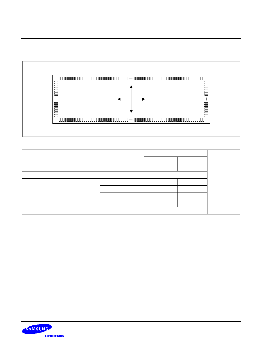
Table 1. Pad Center Coordinates (Continued)
Pad
No.
Pad
N a m e
Coordinate
Pad
No.
Pad
N a m e
Coordinate
Pad
No.
Pad
N a m e
Coordinate
X
Y
X
Y
X
Y
101
S14
4545
1635
135
S48
1485
1635
169
S82
-1575
1635
102
S15
4455
1635
136
S49
1395
1635
170
S83
-1665
1635
103
S16
4365
1635
137
S50
1305
1635
171
S84
-1755
1635
104
S17
4275
1635
138
S51
1215
1635
172
S85
-1845
1635
105
S18
4185
1635
139
S52
1125
1635
173
S86
-1935
1635
106
S19
4095
1635
140
S53
1035
1635
174
S87
-2025
1635
107
S20
4005
1635
141
S54
945
1635
175
S88
-2115
1635
108
S21
3915
1635
142
S55
855
1635
176
S89
-2205
1635
109
S22
3825
1635
143
S56
765
1635
177
S90
-2295
1635
110
S23
3735
1635
144
S57
675
1635
178
S91
-2385
1635
111
S24
3645
1635
145
S58
585
1635
179
S92
-2475
1635
112
S25
3555
1635
146
S59
495
1635
180
S93
-2565
1635
113
S26
3465
1635
147
S60
405
1635
181
S94
-2655
1635
114
S27
3375
1635
148
S61
315
1635
182
S95
-2745
1635
115
S28
3285
1635
149
S62
225
1635
183
S96
-2835
1635
116
S29
3195
1635
150
S63
135
1635
184
S97
-2925
1635
117
S30
3105
1635
151
S64
45
1635
185
S98
-3015
1635
118
S31
3015
1635
152
S65
-45
1635
186
S99
-3105
1635
119
S32
2925
1635
153
S66
-135
1635
187
S100
-3195
1635
120
S33
2835
1635
154
S67
-225
1635
188
S101
-3285
1635
121
S34
2745
1635
155
S68
-315
1635
189
S102
-3375
1635
122
S35
2655
1635
156
S69
-405
1635
190
S103
-3465
1635
123
S36
2565
1635
157
S70
-495
1635
191
S104
-3555
1635
124
S37
2475
1635
158
S71
-585
1635
192
S105
-3645
1635
125
S38
2385
1635
159
S72
-675
1635
193
S106
-3735
1635
126
S39
2295
1635
160
S73
-765
1635
194
S107
-3825
1635
127
S40
2205
1635
161
S74
-855
1635
195
S108
-3915
1635
128
S41
2115
1635
162
S75
-945
1635
196
S109
-4005
1635
129
S42
2025
1635
163
S76
-1035
1635
197
S110
-4095
1635
130
S43
1935
1635
164
S77
-1125
1635
198
S111
-4185
1635
131
S44
1845
1635
165
S78
-1215
1635
199
S112
-4275
1635
132
S45
1755
1635
166
S79
-1305
1635
200
S113
-4365
1635
133
S46
1665
1635
167
S80
-1395
1635
134
S47
1575
1635
168
S81
-1485
1635