 | –≠–ª–µ–∫—Ç—Ä–æ–Ω–Ω—ã–π –∫–æ–º–ø–æ–Ω–µ–Ω—Ç: SI-3050R | –°–∫–∞—á–∞—Ç—å:  PDF PDF  ZIP ZIP |

52
Parameter
DC Input Voltage
Voltage of Rest Signal Output Terminal
DC Output Current
Power Dissipation
Junction Temperature
Ambient Operating Temperature
Storage Temperature
Thermal Resistance (junction to case)
Thermal Resistance (junction to ambient air)
SI-3000R Seires
5-Terminal, Multi-Function, Full-Mold, Low Dropout Voltage Dropper Type with Reset Function
s
Features
∑ Reset signal output (As the output rises it sends a reset signal to the micro-
computer to secure normal operation of the system. As the output drops a
reset signal is also sent out to protect the system.)
∑ Reset signal detection output voltage level Voth is 92% of output voltage in
the standard specification. Models with different setting values for different
needs are scheduled to be added to the series.
∑ Delay time for reset signal can be adjusted freely by external capacitor.
∑ Compact full-mold package (equivalent to TO220)
∑ Output current: 1.5A
∑ Low dropout voltage :V
DIF
1V (at I
O
=1.5A)
Applicable to battery driven equipment with built-in microcomputer.
∑ Built-in droping type overcurrent, overvoltage, thermal protection circuits
∑ Low circuit current I
D
=typ.1.5mA(I
O
=0A)
s
Applications
∑ Microcomputer-controlled equipment
∑ Battery-driven micro-computer-controlled equipment
s
Absolute Maximum Ratings
(T
a
=25
∞
C)
Unit
V
V
A
W
W
∞
C
∞
C
∞
C
∞
C/W
∞
C/W
Symbol
V
IN
V
RST
I
O
P
D1
P
D2
T
j
T
OP
T
stg
R
th(j-c)
R
th(j-a)
Ratings
SI-3050R
35
V
IN
1.5
*1
18(With infinite heatsink)
1.5(Without heatsink, stand-alone operation)
≠30 to +125
≠30 to +105
≠30 to +125
5.5
66.7(Without heatsink, stand-alone operation)
q
SI-3000R Series

53
Parameter
Input Voltage
Output Voltage
Dropout Voltage
Line Regulation
Load Regulation
Ripple Rejection
Quiescent Circuit
Current
Overcurrent Protection Starting
Current (Drooping Type)
Limited Current at Overcurrent
Protection Operation
DLY
Threshold
Terminal Source
Reset Threshold Voltage Level
(Voth: Threshold Output Voltage)
Reset Threshold Voltage Hysteresis
H-level Output Voltage
L-level Output Voltage
Sink Current at H level
Source Current at L level
s
Electrical Characteristics
*1: V
IN(max)
and I
O(max)
are restricted by the relation P
D(max)
=(V
IN
-V
O
)∑I
O
=18(W).
*2: Refer to the dropout voltage.(Refer to Setting D
C
Input Voltage on page 7.)
*3: I
S
1 is specified at ≠5(%) drop point of output voltage V
O
on the condition that V
IN
=8V, I
O
=1.0A.
*4: Reset signal output terminal V
RST
is an open-collector output. Use a pull-up resistor when connecting it to a logic circuit.
Unit
V
V
V
mV
mV
dB
mA
A
A
V
µ
A
%
mV
V
V
µ
A
mA
Symbol
V
IN
V
O
Conditions
V
DIF
Conditions
Conditions
V
OLINE
Conditions
V
OLOAD
Conditions
R
REJ
Conditions
I
q
Conditions
I
S1
Conditions
I
S2
Conditions
V
DLyth
I
DLY
V
oth
/V
O
V
oth
V
RSTH
V
RSTL
I
RSTH
I
RSTL
Ratings
SI-3050R
min.
typ.
max.
6
*2
30
*1
4.80
5.00
5.20
V
IN
=8V, I
O
=1.0A
0.5
I
O
1.0A
1.0
I
O
1.5A
30
V
IN
=6 to 15V, I
O
=1.0A
100
V
IN
=8V, I
O
=0 to 1.5A
54
V
IN
=8V, f=100 to 120H
Z
1.5
5.0
V
IN
=8V, I
O
=0A
1.6
V
IN
=8V
1.6
V
IN
=8V
2.7
2.9
3.1
25
35
45
90
92
94
50
100
150
V
CC
≠1
0.8
≠20
≠16
(T
a
=25
∞
C unless otherwise specified)
q
SI-3000R Series
V
RST
Terminal*4
54
s
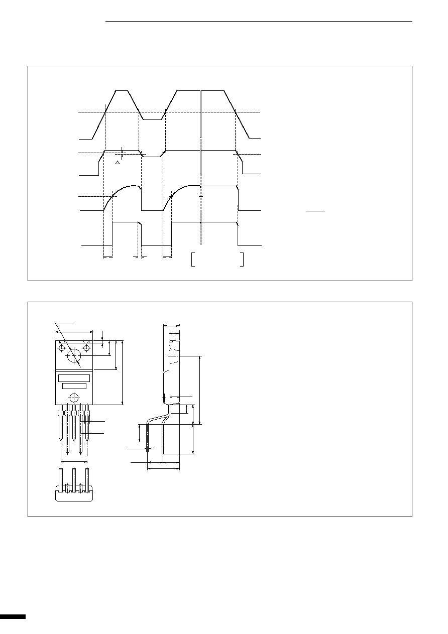
Reset Signal Output Timing Chart
Terminal Connections
q
GND
w
DELAY
e
V
O
r
Rest Signal output
t
V
IN
Plastic Mold Package Type
Flammability: UL94V-0
Weight: Approx. 2.3g
s
Outline Drawing
GND
GND
O(V)
O(V)
V
O
+V
DIF
V
oth
V
DLY
th
V
oth
V
DLY
V
RSTH
t
DLY
t
DLY
t
RESET (mim.)
V
RSTL
V
O
V
IN
Input Voltage
Output Voltage
Voltage Across
Delay Capacitor
Reset Signal Output
Vo drops for a period
less than t
RESET
(min)
The delay time
tDLY
of the reset signal can
be calculated from the following formula:
t
DLY
=
V
DLYth
◊
C
DLY
I
DLY
*I
DLY
is the current flowing from the
DLY
terminal shown in the standard connec-
tion circuit diagram.
(unit:mm)
q
SI-3000R Series
10.0
±
0.2
4.2
±
0.2
0.95
±
0.15
8.2
±
0.7
2.6
±
0.1
3.9
±
0.7
(4.3)
(4.6)
(8.0)
(17.9)
(2.0)
0.85
+0.2
≠0.1
0.45
+0.2
≠0.1
3.2
±
0.2
4.0
±
0.2
7.9
±
0.2
5.0
±
0.6
16.9
±
0.3
0.5
1 2 3 4 5
P1.7
±
0.7
◊
4=6.8
±
0.7
2.8
±
0.2
Forming No. 1101
Part Number
Lot Number
55
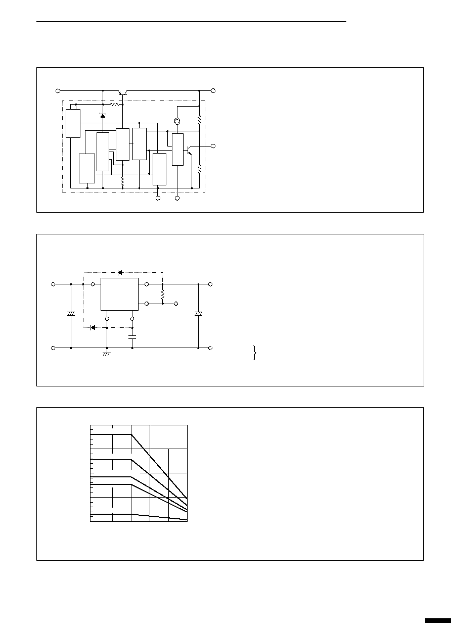
s
Block Diagram
s
Standard External Circuit
C
0
: Output capacitor (Approx. 200
µ
F)
*1 C
1
: Oscillation prevention capacitor (C
1
: Approx. 47
µ
F)
The distance between terminals No.5 (V
IN
) and No.1 (GND)
must be made as short as possible. If the input line is induc-
tive or in the case of long wiring, a capacitor of approxi-
mately 0.33
µ
F with superior high frequency characteristics
must be connected in parallel. Tantalum capacitors are rec-
ommended for C
1
and C
0
, particularly at low temperatures.
*2 C
DLY
: Delay capacitor (reset output)
*3 R
1
: Pull-up resistor (300
or above)
*4 D
1
: Protection diodes
These diodes are required for protection against reverse
biasing of the input and output. Sanken EU2Z is recom-
mended.
s
T
a
-P
D
Characteristics
P
D
=I
O
∑[V
IN
(mean)≠V
O
]
5
T
r1
3
1
MIC
4
2
Drive
Amp.
Reset
Reg.
TSD
OCP, OVP
V
REF
q
SI-3000R Series
D
2
*
4
D
1
3
4
5
1
2
D
2
*
4
C
1
*
1
R
1
*
3
*
2
C
DLY
C
0
+
+
SI-3050R
DC Input
V
O
DC Output
V
O
Reset Signal
Output Terminal
15
20
10
5
0
≠30
0
25
50
Ambient Temperature T
a
(
∞
C)
Power Dissipation P
D
(W)
75
100
75
◊
75
◊
2mm (7.6
∞
C/W)
100
◊
100
◊
2mm (5.2
∞
C/W)
200
◊
200
◊
2mm (2.3
∞
C/W)
Infinite heatsink
Without heatsink
With Silicon Grease
Heatsink: Aluminum
56
s
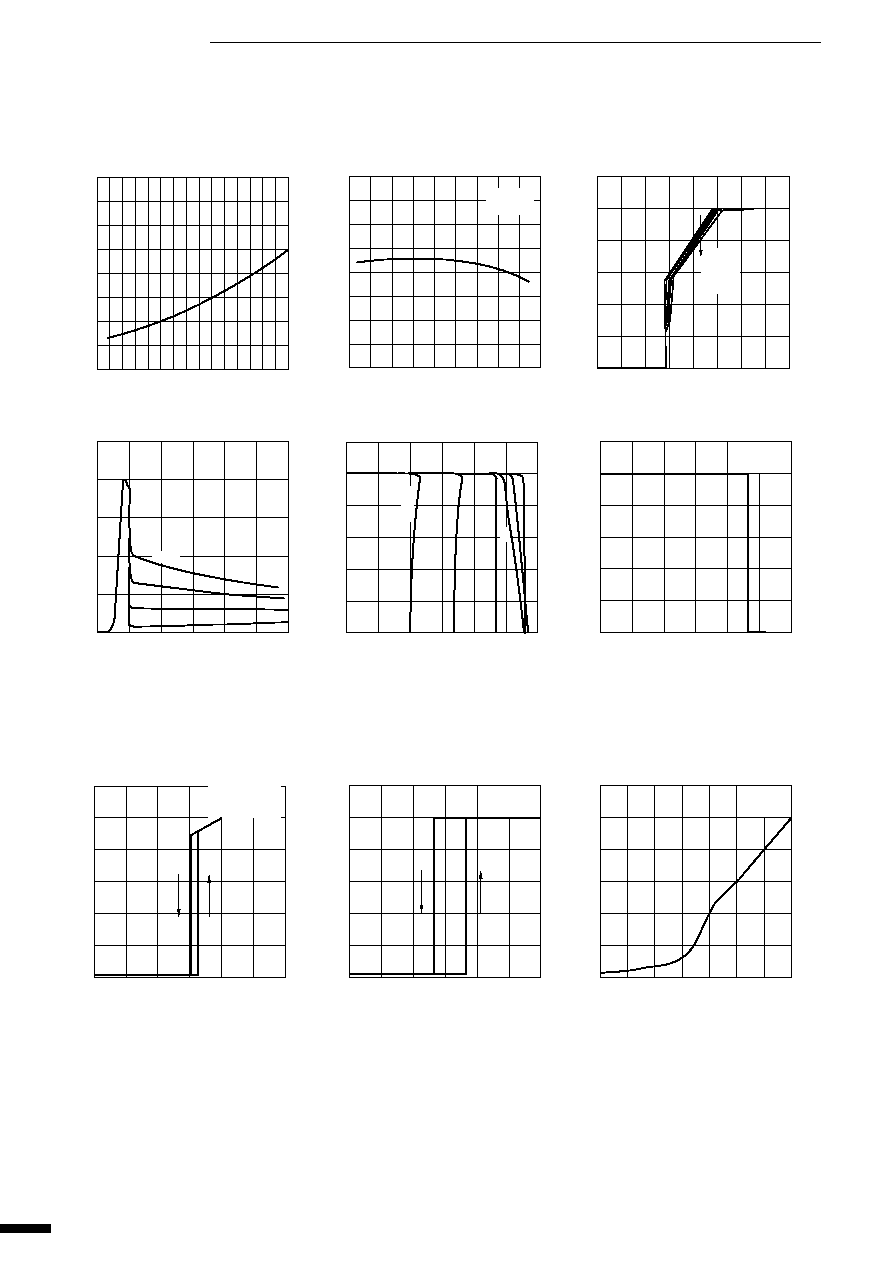
Typical Characteristics
I
O
vs. V
DIF
Characteristics
Temperature Coefficient of Output Voltage
Rise Characteristics
Circuit Current
Overcurrent Protection Characteristics
Thermal Protection Characteristics
Reset Output vs. V
O
Characteristics
Reset Output vs. DLY Terminal Voltage Characteristics
Reset Signal Delay Time tDLY(sec)
≠40 ≠20
0
20
40
60
80
100 120 140
5.06
5.04
5.02
5.00
4.98
4.96
4.94
4.92
4.90
Ambient Temperature T
a
(
∞
C)
Output Voltage V
O
(V)
V
IN
=8V
l
O
=10mA
0
0.5
1
1.5
2
2.5
3
6
5
4
3
2
1
0
Output Current l
O
(A)
Output Voltage V
O
(V)
V
IN
=30V
25V
20V
6V
15V
8V
60
80
100
120
140
160
180
6
5
4
3
2
1
0
Case Temperature T
C
(
∞
C)
Output Voltage Vo (V)
V
IN
=8V
l
O
=10mA
1.0
1.5
2.0
2.5
3.0
3.5
4.0
6
5
4
3
2
1
0
DLY Terminal Voltage V
DLY
(V)
Reset Output Voltage V
RST
(V)
V
IN
=8V l
O
=0A
R
L
=510
1p
10p
100p 1000p 0.01
µ
0.1
µ
1
µ
10
µ
10
1
100m
10m
1m
100
µ
10
µ
Delay Capacitor Capacitance C
DLY
(F)
Delay Time t
DLY
(sec.)
V
IN
=8V
l
O
=0A
3.0
3.5
4.0
4.5
5.0
5.5
6.0
Output Voltage V
O
(V)
6
5
4
3
2
1
0
V
IN
=8V l
O
=0A
R
L
=510
Reset Output Voltage V
RST
(V)
(T
a
=25
∞
C)
q
SI-3000R Series
Note on Thermal Protection:
The thermal protection circuit is intended for pro-
tection against heat during instantaneous short-
circuiting. Its operation is not guaranteed for short-
circuiting over extended periods of time.
0
0.5
1.0
1.5
0.8
0.6
0.4
0.2
0
Output Current lo (A)
Dropout Voltage V
DIF
(V)
0
1
2
3
4
5
6
7
8
6
5
4
3
2
1
0
Input Voltage V
IN
(V)
Output Voltage V
O
(V)
l
O
=0A
0.5A
1A
1.5A
0
5
10
15
20
25
30
25
20
15
10
5
0
Input Voltage V
IN
(V)
Ground Current I
G
(mA)
l
O
=1.5A
1A
0.5A
0A