Parameter
Symbol
Unit
Conditions
Ratings
Absolute Maximum Ratings
Electrical Characteristics
Parameter
Symbol
min
typ
max
Unit
Conditions
Ratings
(Ta=25ЇC)
Power supply voltage
Input terminal voltage
DIAG terminal voltage
Collector-emitter voltage
Power Dissipation
Input voltage
Input current
Operating power supply voltage
Quiescent circuit current
Thermal protection starting
temperature
Minimum load inductance
Open load detection resistor
Output transfer time
DIAG output voltage
DIAG output transfer time
(Ta=25ЇC unless otherwise specified)
Saturation voltage of output
transistor
Junction temperature
Operating temperature
Storage temperature
V
B
V
IN
V
DIAG
V
Bopr
V
Bopr
= 14V, V
IN
= 0V
I
O
1.0A, V
Bopr
= 6 to 16V
I
O
1.8A, V
Bopr
= 6 to 16V
V
Bopr
= 6 to 16V
V
Bopr
= 6 to 16V
V
IN
= 5V
V
IN
= 0V
V
Bopr
= 14V, V
O
= V
Bopr
≠1.5V
V
Bopr
= 6 to 16V
V
Bopr
= 14V, I
O
= 1A
V
Bopr
= 14V, I
O
= 1A
V
CC
= 6V
V
CC
= 6V, I
DD
= 2mA
V
Bopr
= 14V, I
O
= 1A
V
Bopr
= 14V, I
O
= 1A
V
5
12
6.0
30
mA
0.5
V
1.0
V
V
B
V
0.8
V
1
mA
145
30
8
30
15
30
6
0.3
30
30
mA
125
ЇC
k
µ
S
µ
S
V
V
µ
S
µ
S
Iq
Output leak current
V
CEO
= 16V
2.0
≠0.3
≠0.1
2
mA
I
O
, leak
V
CE (sat)
V
IH
V
IL
I
IH
I
IL
T
TSD
Overcurrent protection starting
current
1.9
A
I
S
Ropen
T
ON
T
OFF
4.5
1
V
DH
V
DL
T
PLH
T
PHL
mH
L
V
CE
P
D1
P
D2
Tj
T
OP
Tstg
Output ON
Output OFF
Output ON
Output OFF
V
V
With infinite heatsink (Tc
= 25ЇC)
Stand-alone without heatsink
(Tc
= 25ЇC)
V
V
W
W
ЇC
ЇC
ЇC
40
≠0.3 to V
B
6
40
Output current
I
O
A
1.8
18
1.5
≠40 to +125
≠40 to +100
≠40 to +125
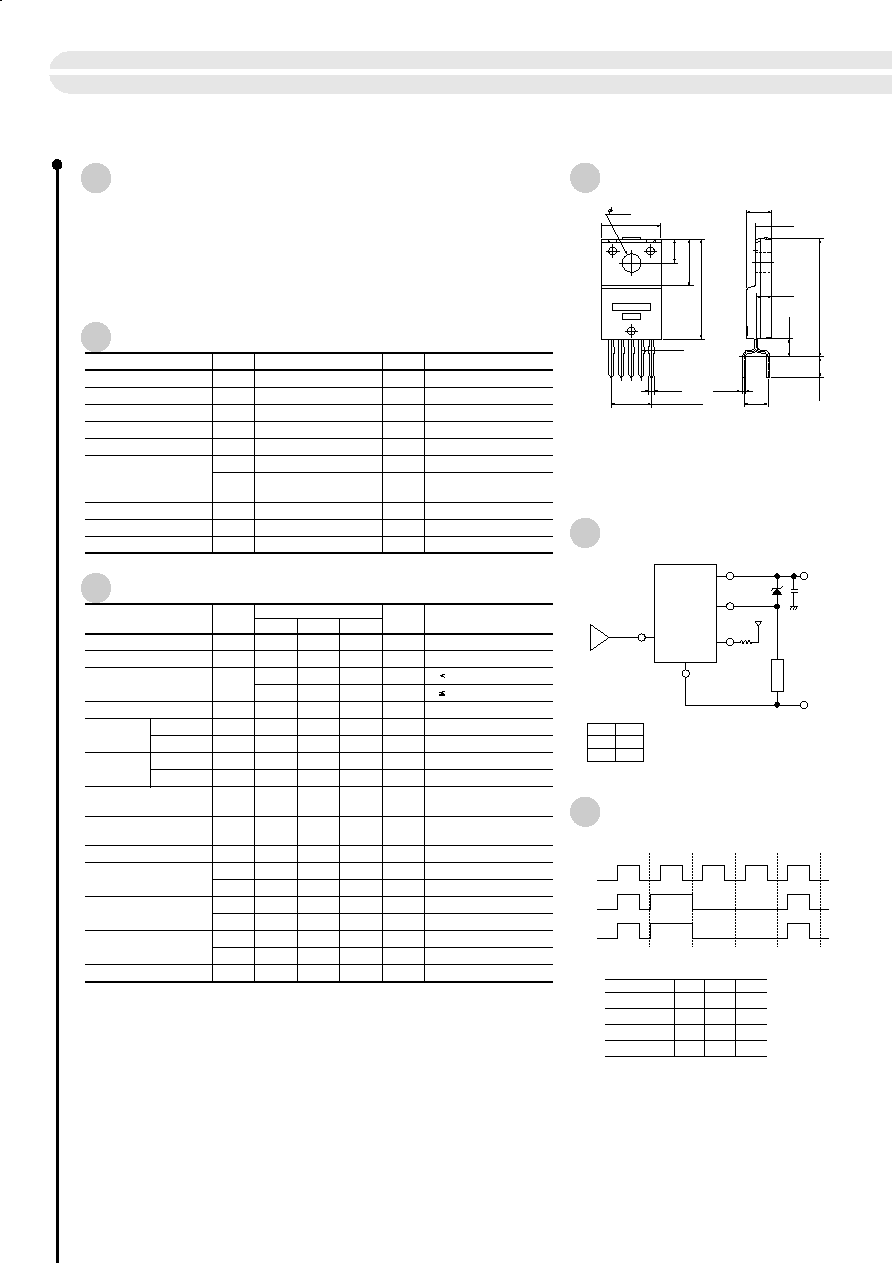
Standard Circuit Diagram
Diagnostic Function
External Dimensions
(unit: mm)
Features
q Built-in diagnostic function to detect short and open circuiting of loads and
output status signals
q Low saturation PNP transistor use
q Allows direct driving using LS-TTL and C-MOS logic levels
q Built-in overcurrent and thermal protection circuits
q Built-in protection against reverse connection of power supply
q TO-220 equivalent full-mold package not require insulation mica
SI-5151S
P
Z
DIAG
5.1k
GND
1
4
3
5
2
V
IN
V
IN
V
O
H
H
L
L
V
O
V
CC
V
B
Load
LS-TTL
or
CMOS
V
IN
V
O
DIAG
Normal
Normal
Open load
Overheat
Shorted load
Truth table
1. GND
2. V
IN
3. V
O
4. DIAG
5. V
B
a: Type No.
b: Lot No.
(Forming No. 1123)
V
IN
DIAG
Open load
Normal
Mode
Shorted load
Overheat
L
H
V
O
L
H
L
H
L
H
H
H
H
H
L
H
L
L
L
L
L
H
L
L
L
L
q DIAG output will be undetermined when a voltage
exceeding 25V is applied to V
B
terminal.
Note:
* The rule of protection against reverse connection of power supply is V
B
= ≠13V, one minute
(all terminals except, V
B
and GND, are open).
20
High-side Power Switch with Diagnostic Function SI-5151S
10
2.6
4.2
2.8
3.2
4
7.9
20
max
3.6
16.9
P1.7 Ј 4 = 6.8
0.94
4
0.85
0.45
+0.2
≠0.1
+0.2
≠0.1
2.9
R-end
±
0.5
±
0.6
±
0.1
±
0.2
±
0.2
±
0.2
±
0.2
±
0.15
±
0.1
±
0.2
±
0.3
±
0.2
+0.2 ≠
0.3
a
b

0
0
10
5
10
20
30
40
--40ЇC
95ЇC
25ЇC
I
q
(mA)
V
B
(V)
V
B
(V)
0
0
10
10
20
30
40
20
30
T --40
ЇC
=
T 25
ЇC
=
T 95
ЇC
=
40
50
I
B
(mA)
0
0
1
2
3
0.5
1.0
95
ЇC
V =
6 to 16V
B
--40
ЇC
25
ЇC
V
CE
(sat)
(V)
I
O
(A)
0
0
1
2
3
16
10
14V
V =
B
2
4
6
8
12
14
V
O
(V)
I
O
(A)
0
0
1
2
3
16
10
8
14V
V =
B
12
14
4
2
6
I
O
(A)
V
O
(V)
0
0
1
2
3
16
10
2
14V
V =
B
14
12
4
6
8
V
O
(V)
I
O
(A)
0
0
1
2
10
20
15
5
2.2
95
ЇC
T
a
=
25
ЇC
≠40
ЇC
16V
=
B
V
1A
=
O
I
V
IN
(V)
V
O
(V)
≠40
0
0
50
0.5
1.0
100
Ta (ЇC)
I
IH
(mA)
14V
=
B
V
5V
=
IN
V
≠40
0
50
100
Ta (ЇC)
0
0.2
0.1
14V
=
B
V
V
DG
(sat)
(V)
≠40
0
0
50
100
Ta (ЇC)
I
IL
(
µ
A)
14V
=
B
V
0V
=
IN
V
1
2
0
50
100
Ta (ЇC)
0
150
10
16
2
4
6
8
12
14
2
4
6
DIAG (V)
1
3
5
V
O
(V)
Vo
DIAG
14V
=
B
V
10mA
=
O
I
a
a
a
21
s
Quiescent Circuit Current
s
Circuit Current
s
Saturation Voltage of Output Transistor
s
Overcurrent Protection Characteristics
(Ta=25ЇC)
s
Overcurrent Protection Characteristics
(Ta=100ЇC)
s
Input Current
(Output OFF)
s
Input Current
(Output ON)
s
Threshold input voltage
s
Overcurrent Protection Characteristics
(Ta= ≠40ЇC)
s
Saturation Voltage of DIAG Output
s
Thermal Protection Characteristics