Parameter
Symbol
Unit
Conditions
Ratings
Absolute Maximum Ratings
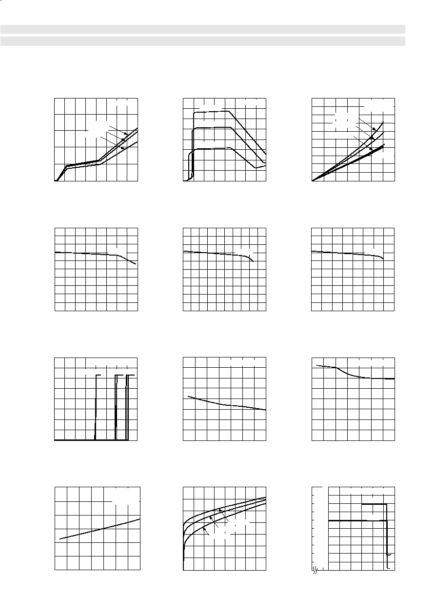
Electrical Characteristics
Parameter
Symbol
min
typ
max
Unit
Conditions
Ratings
(Ta=25∫C)
Power supply voltage
Input terminal voltage
DIAG output applied voltage
Voltage across power supply
and output terminal
Power Dissipation
Input voltage
Operating power supply voltage
Quiescent circuit current (per circuit)
Thermal protection starting
temperature
Open load detection resistor
Output transfer time
DIAG output transfer time
(V
Bopr
=14V, Tj= ≠40 to +150∫C unless otherwise specified)
Junction temperature
Operating temperature
Storage temperature
V
B
V
IN
V
DIAG
V
Bopr
Lo output
Tj
= 25∫C
V
O
= V
Bopr
≠1.5V
V
Bopr
6V
I
O
= 1A
I
O
= 1A
I
O
= 1A
I
O
= 1A
V
0.8
19.3
1.0
2.5
34
34
1.6
6.0
16
mA
1.5
V
30
100
30
100
60
V
∫C
k
µ
S
µ
S
µ
S
µ
S
Iq
Circuit current (per circuit)
mA
I
B
0.8
3.7
Threshold input voltage
3.0
V
V
IN
th
V
IN
V
IN
T
TSD
Overcurrent protection starting
current
1.6
5.5
Minimum load inductance
mH
Lo
1.0
Maximum ON duty
%
D
(ON)
0
A
I
S
Ropen
Leak current of DIAG output
V
CC
= 7V
≠100
µ
A
I
DGH
Saturation voltage of DIAG output
I
DGH
= ≠2mA, V
Bopr
= 6 to 16V
0.4
V
V
DL
Saturation voltage of output
transistor
I
O
1.2A, V
Bopr
= 6 to 16V
0.2
V
V
CE (sat)
I
O
1.5A, V
Bopr
= 6 to 16V
V
V
CE (sat)
Output terminal sink current
Tj
= 25∫C, V
CEO
= 14V
5
mA
I
O (off)
Surge clamp voltage
Tj
= 25∫C, I
C
= 10mA
39
V
V
B≠O
I
C
= 5mA
40
V
T
ON
T
OFF
T
PLH
T
PHL
V
B≠O
P
D
Tj
T
OP
Tstg
Hi output
Lo output
Input current
V
IN
= 5V
V
IN
= 0V
100
29
28
≠1.0
mA
µ
A
I
IN
I
IN
Hi output
Lo output
V
V
Stand-alone without heatsink,
all circuits operating
C
= 200pF, R
= 0
V
V
W
∫C
∫C
∫C
≠13 to +40
≠0.3 to +7.0
Drive terminal applied voltage
V
D
V
≠0.3 to V
B
≠0.3 to +7.0
DIAG output source current
I
DIAG
mA
≠3
V
B
≠34
Voltage across power supply
and drive terminal
V
B≠D
V
≠0.4
Output current
I
O
A
1.5
Output reverse current
I
O
A
≠1.8
Electrostatic resistance
E
S/A
V
±
250
4.8
≠40 to +150
≠40 to +115
≠50 to +150
Note:
* The Zener diode has an energy capability of 200 mJ (single pulse).
* A start failure may occur if a short OFF signal of 10 ms or below is input in the V
IN
terminal.
Equivalent Circuit Diagram
Standard Circuit Diagram
Diagnostic Function
External Dimensions
(unit: mm)
Features
q Built-in diagnostic function to detect short and open circuiting of loads and
output status signals
q Low saturation PNP transistor use (V
CE (sat)
0.2V)
q Allows direct driving using LS-TTL and C-MOS logic levels
q Built-in Zener diode in transistor eliminates the need of (or simplifies) external
surge absorption circuit
q Built-in independent overcurrent and thermal protection circuit in each circuit
q Built-in protection against reverse connection of power supply
q Tj = 150∫C guaranteed
V
IN
V
O
V
DIAG
Normal
Normal
Open load
Overheat
Shorted load
V
IN
V
B
OUT
D
FLT
GND
MIC
a
c
f
b
d
g
e
SLA2501M
GND
1
OUT
1
OUT
2
OUT
3
FLT
1
IN
1
IN
2
V
B
V
B
V
CC
D
1
D
2
D
3
IN
3
FLT
2
FLT
3
GND
2
5
7
12
6
11
2
10
15
1
3
9
14
4
8
13
a: Type No.
b: Lot No.
31
Ellipse 3.2
∑
3.8
14 ∑ P2.03 = (28.42)
24.4
4.8
1.7
2.45
0.65
3.2
12.9
16
9.9
6.4
0.55
1.15
+0.2
≠0.1
+0.2
≠0.1
+0.2
≠0.1
31.3
1 2 3
15
a
b
3-circuit High-side Power Switch Array SLA2501M
32
a: Pre-regulator
b: Overvoltage protection circuit
c: Control circuit
d: Driver circuit
e: Overcurrent protection circuit
f: Diagnostic circuit
g: Thermal protection circuit
±
0.1
±
0.2
±
0.2
±
0.15
±
0.2
±
0.2
±
0.2
±
0.2
±
0.5
±
0.2
±
0.1
±
0.2
±
0.15