70
Characteristic curves
SLA5040
(T
a
=25
∞
C)
Symbol
Unit
Conditions
V
(BR)DSS
100
V
I
D
=250
µ
A, V
GS
=0V
I
GSS
±
500
nA
V
GS
=
±
20V
I
DSS
250
µ
A
V
DS
=100V, V
GS
=0V
V
TH
2.0
4.0
V
V
DS
=10V, I
D
=250
µ
A
Re
(
yfs
)
1.1
1.7
S
V
DS
=10V, I
D
=4A
R
DS(ON)
0.50
0.60
V
GS
=10V, I
D
=4A
Ciss
180
pF
V
DS
=25V, f=1.0MHz,
Coss
82
pF
V
GS
=0V
t
on
40
ns
I
D
=4A, V
DD
=50V, V
GS
=10V,
t
off
40
ns
see Fig. 3 on page 16.
V
SD
1.2
2.0
V
I
SD
=4A, V
GS
=0V
t
rr
250
ns
I
SD
=
±
100mA
(T
a
=25
∞
C)
Symbol
Ratings
Unit
V
DSS
100
V
V
GSS
±
20
V
I
D
±
4
A
I
D(
pulse
)
±
8 (PW
1ms)
A
E
AS
*
16
mJ
I
F
4 (PW
0.5ms, Du
25%)
A
I
FSM
8 (PW
10ms, Single pulse)
A
V
R
120
V
P
T
5
(Ta=25
∞
C, with all circuits operating, without heatsink)
W
35 (Tc=25
∞
C,
with all circuits operating, with infinite heatsink
)
W
j-a
25 (Junction-Air, Ta=25
∞
C, with all circuits operating)
∞
C/W
j-c
3.57 (Junction-Case, Tc=25
∞
C, with all circuits operating)
∞
C/W
V
ISO
1000 (Between fin and lead pin, AC)
Vrms
Tch
150
∞
C
Tstg
≠40 to +150
∞
C
* : V
DD
=20V, L=1mH, I
D
=5A, unclamped, see Fig. E on page 15.
Specification
min
typ
max
Symbol
Unit
Conditions
V
R
120
V
I
R
=10
µ
A
V
F
1.0
1.2
V
I
F
=1A
I
R
10
µ
A
V
R
=120V
t
rr
100
ns
I
F
=
±
100mA
q
Diode for flyback voltage absorption
Specification
min
typ
max
1
2
5
4
6
3
8
9
12
11
10
7
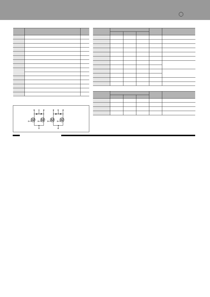
N-channel
With built-in flywheel diode
Absolute maximum ratings
Electrical characteristics
s
Equivalent circuit diagram
External dimensions
A
∑ ∑ ∑
SLA