Parameter
Symbol
Unit
Conditions
Ratings
Absolute Maximum Ratings
Electrical Characteristics
Parameter
Symbol
min
typ
max
Unit
Conditions
Ratings
(Ta=25∫C)
Power supply voltage
Input terminal voltage
Power Dissipation
Input voltage
Power supply voltage
Quiescent circuit current
Overcurrent protection starting
current
Forward voltage of output stage
diode
Output transfer time
(V
B
=14V, Ta=25∫C unless otherwise specified)
Storage temperature
Channel temperature
Output avalanche capability
V
B
V
IN
V
Bopr
V
IN
= 0V (all inputs)
I
O
= 1A
R
L
= 14
, I
O
= 1A
R
L
= 14
, I
O
= 1A
R
L
= 14
, I
O
= 1A
R
L
= 14
, I
O
= 1A
V
5
0.4
0.5
0.6
0.7
50
7
5.5
25
mA
1.5
5.5
V
12
8
10
5
V
A
V
µ
s
µ
s
Iq
Operating circuit current
V
IN
= 5V (all inputs)
8
12
mA
I
CC
3.5
≠0.5
V
IN
V
IN
I
S
Thermal protection starting
temperature
151
165
1.1
41
Output rise time
µ
s
T
r
Output fall time
µ
s
T
f
∫C
T
TSD
Overvoltage protection starting
voltage
25
V
V
B (ovp)
V
F
Output leak current
V
O
= 37V
I
F
= 0.5A
10
1.6
40
µ
A
I
OH
Output clamp voltage
I
O
= 1A
55
V
V
OUT (clamp)
Output ON resistance
30
R
DS (ON)
V
B
= 5.5V
T
ON
T
OFF
P
D
Tstg
Tch
E
AV
Hi output
Lo output
Input current
V
IN
= 5V
V
IN
= 0V
50
µ
A
µ
A
I
IN
I
IN
Hi output
Lo output
V
V
W
∫C
∫C
mJ
Single pulse
40
≠0.5 to +7.5
Output terminal voltage
V
OUT
V
37
Output current
I
O
A
1.8
2
≠40 to +150
150
50
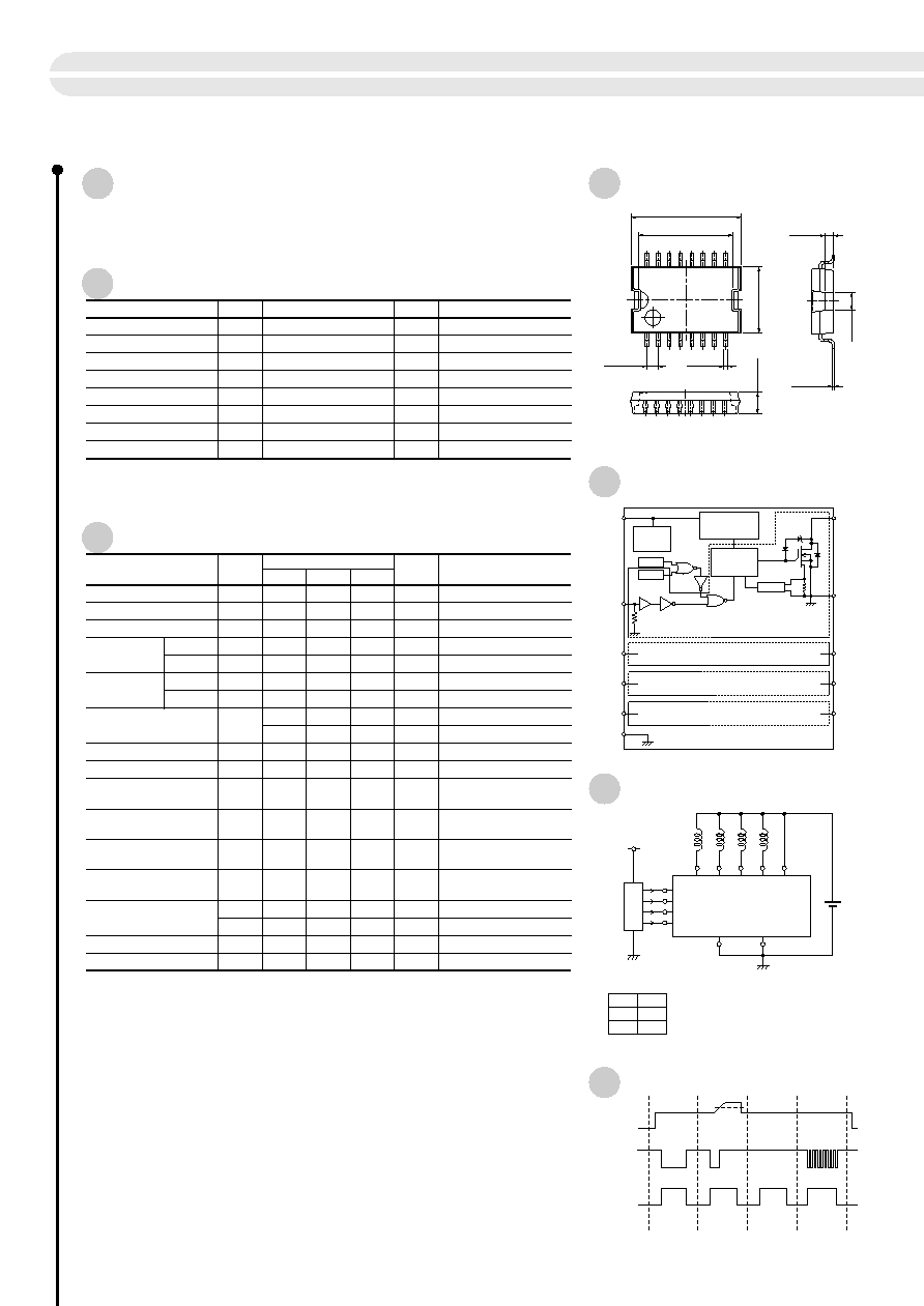
Equivalent Circuit Diagram
Circuit Example
Timing Chart
External Dimensions
(unit: mm)
Features
q DMOS 4ch output
q Allows ON/OFF using C-MOS logic level
q Built-in overcurrent, overvoltage and thermal protection circuits
Low-side Switch ICs
[Surface-mount 4-circuits]
SPF5002A
40
12.2
1.0
2.5
7.5
10.5
1.27
16
1
8
9
0.4
+0.15
≠0.05
+0.1
≠0.05
+0.15
≠0.05
+0.2 ≠
0.8
0.25
2.0
Fin
thickness
V
B
V
OUT
1
V
IN
1
V
IN
2
V
IN
3
V
IN
4
V
OUT
2
V
OUT
3
V
OUT
4
L-GND
P-GND
Reg. REF
OVP
TSD
250 k
typ
Gate Protction
Gate Driver
OCP
Use L-GND and P-GND being connected.
V
B
V
OUT
V
IN
OVP
Normal
Overvoltage
Overheat
Overcurrent
* Self-excited frequency is used in the overcurrent protection.
V
IN
V
O
H
L
L
H
Truth table
±
0.2
±
0.25
±
0.2
±
0.2
±
0.2
V
CC
V
B
4
6
12
14
IN1
OUT1 OUT3
OUT2 OUT4
IN2
IN3
IN4
L-GND
P-GND
CONTROL
UNIT
13
1,9
SPF5002A
2
10
7
15
5

41
s
Quiescent Circuit Current
0
10
20
30
40
0
4
8
Iq (mA)
V
B
(V)
6
2
10
0
4
8
6
2
10
0
4
8
6
2
10
s
Circuit Current (single circuit)
0
10
20
30
40
Id (mA)
V
B
(V)
s
Threshold Input Voltage
0
1
2
3
0
5
10
V
O
(V)
V
IN (th)
(V)
15
s
Overcurrent Protection Characteristics
0
1.0
2.0
0
V
O
(V)
I
O
(A)
10
5
15
s
Forward Voltage of Output Stage Diode
0
0.5
1.0
1.5
0
0.5
1.5
I
F
(A)
V
F
(V)
1.0
s
Output ON Voltage
0
0.5
1.0
1.5
2.0
0
0.4
0.8
V
DS (ON)
(V)
I
O
(A)
0.6
0.2
1.0
s
Circuit Current (4 circuits)
10
20
30
40
Id (mA)
V
B
(V)
s
Overvoltage Protection Starting Voltage
0
10
20
30
40
0
V
O
(V)
V
B
(V)
10
5
15
Ta
= 120∫C
Ta
= 25∫C
Ta
= ≠40∫C
Ta
=
125
∫C
Ta
= 25∫C
Ta
= ≠40∫C
Ta
= 25∫C
Ta
= ≠40∫C
Ta
= 125∫C
V
O
=
14V
I
O
=
0.1A
Ta
= ≠40∫C
Ta
= 125∫C
Ta
= 25∫C
V
B
= 14V
Ta
= 125∫C
Ta
= 25∫C
Ta
= ≠40∫C
V
B
=14V
Ta
= 120∫C
Ta
= 25∫C
Ta
= ≠40∫C
I
O
=
0.1A
Ta
= ≠40∫C
Ta
= 25∫C
Ta
= 125∫C
Electrical Characteristics
Ta
= ≠40∫C
Ta
= 25∫C
Ta
= 125∫C
SPF5002A