Parameter
Symbol
Unit
Conditions
Ratings
Absolute Maximum Ratings
Electrical Characteristics
Parameter
Symbol
min
typ
max
Unit
Conditions
Ratings
(Ta=25∫C)
Power supply voltage
Input terminal voltage
Input terminal current
DG terminal voltage
Input threshold
voltage
Inpup current
Operating power supply voltage
Quiescent circuit current
Thermal shutdown operating temperature
Load open detection threshold voltage
DG leak current
Low level DG output voltage
Output transfer time
DG output transfer time
(V
B
=14V, Ta=25∫C unless otherwise specified)
Output ON resistance
Channel temperature
Operating temperature
Storage temperature
V
B
V
IN
I
IN
V
B (opr)
V
IN
=0V, V
OUT
=0V
I
O
=1A
I
O
=1A, Ta=80∫C
Ta= ≠40 to +105∫C
Ta= ≠40 to +105∫C
V
IN
=5V
V
IN
=0V
V
OUT
=V
O
≠1.5V
V
OUT
=0V
R
L
=14
, V
OUT
=V
B
≠5V
R
L
=14
, V
B
∑10%
V
DG
=5.5V
I
DG
=1.6mA
V
50
2.0
1.8
70
1
5.5
35
mA
200
m
350
m
3.0
V
V
200
12
µ
A
165
5
3
4.5
70
3
140
35
0.15
70
45
90
20
0.5
140
120
µ
A
155
1.5
∫C
A
V
µ
s
µ
s
µ
A
V
µ
s
Iq
Output leak current
V
OUT
=0V
1.4
1.0
100
µ
A
I
O
, leak
R
DS (ON)
V
IHth
V
ILth
I
IH
I
IL
T
TSD
Overcurrent protection starting current
Internal current limit
1.9
A
I
S
I
Lim
Vopen
T
ON
T
OFF
V
DGL
I
DG
T
PLH
T
PHL
µ
s
V
DG
V
DS
I
O
P
D
I
F
Tch
T
OP
Tstg
Output ON
Output OFF
Output ON
Output OFF
V
V
Ta=25∫C, all circuit operating
mA
V
V
A
W
A
∫C
∫C
∫C
35
≠0.3 to 7
5
≠0.3 to 7
DG terminal current
Drain to source voltage
Output current
Power dissipation
Source to drain Di forward current
I
DG
mA
5
V
B
≠45
1.8
2.7
0.8
150
≠40 to +105
≠40 to +150
Parameter
Unit
Ratings
Recommended Operating Conditions (for one channel)
Power supply voltage
V
IH
V
IL
I
O
R
IN
R
DG
5.5
4
≠0.3
10
10
16
5.5
0.9
1
20
20
V
V
V
A
k
k
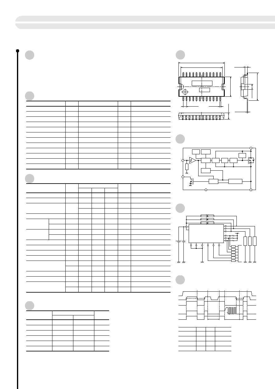
External Dimensions
(unit: mm)
Features
q Built-in diagnostic function to detect short and open circuiting of loads and
output status signals
q DMOS 3ch output
q Allows ON/OFF using C-MOS logic level
q Built-in overcurrent and thermal protection circuits
34
High-side Power Switch ICs
[Surface-mount 3-circuits]
SPF5007
(under development)
min
max
Block Diagram (for one channel)
Standard Connection Diagram
Timing Chart
IN
DG
V
B
GND
OUT
Thermal
Protect
Input
Logic
Lavel
Shifting
DG
Logic
Open/Short
Sense
Charge
Pump
Current
Limit
Clamp
Chopper
Bias
IN2
IN3
IN1
GND1
2
13 V
B
1
7
17
18
3
8
5,6
10,11
20,21
4
5V
9
19
GND2
GND3
C
P
U
SPF5007
R
DG
DG1
OUT1
OUT2
OUT3
DG2
DG3
R
DG
R
DG
R
IN
R
IN
R
IN
*
R
IN
and R
DG
are needed to protect CPU and SPF5007 in case of reverse
connection of V
B
terminal.
*
Make V
B
of 1Pin and 13Pin short from the fin to be plated by solder.
1.0
10.5
±
0.3
+0.1
≠0.05
0.25
+0.15
≠0.05
2.0
+0.2 ≠
0.8
Fin
thickness
17.28
±
0.2
2.5
±
0.2
7.5
±
0.2
15.58
±
0.2
1.27
±
0.25
24
1
12
13
0.4
+0.15
≠0.05
a
b
a: Part No.
b: Lot No.
Load
Load
Load
V
B
V
IN
ON
V
IN
OFF
V
O
open
OCP
TSD
Normal
Normal
Over-
heat
Normal
Normal
Normal
Shorted load
Open load
High inpidance
Internal current limit
TSD
ON
TSD
OFF
V
IN
V
OUT
I
OUT
DG
V
IN
DG
Open load
Normal
Mode
Shorted load
Overheat
H
L
V
O
H
L
H
L
H
L
H
H
H
H
H
L
L
L
L
L
(Limiting)
H
L
L
L
L
L