Specifications and information herin are subject to change without notice.
HD 010711
Absolute Maximum Ratings / Ta=25
∞
C
Drain to Source Voltage
Gate to Source Voltage
Drain Current(DC)
Drain Current(Pulse)
Allowable power Dissipation
Channel Temperature
Storage Temperature
*) : Chip Performance Shown
V
V
A
A
W
°C
°C
Electrical Characteristics / Ta=25
∞
C
Drain to Source Breakdown Voltage
Zero Gate Voltage Drain Current
Gate to Source Leakage Current
Cutoff Voltage
Forward Transfer Admittance
Static Drain to Source
On State Resistance
Input Capacitance
Output Capacitance
Reverse Transfer Capacitance
Total Gate Charge
Turn-ON Delay Time
Rise Time
Turn-OFF Delay Time
Fall Time
Diode Forward Voltage
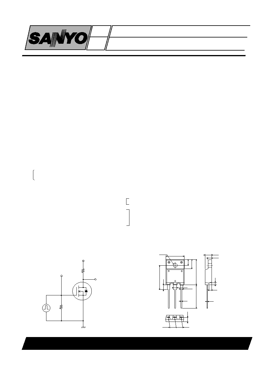
Switching Time Test Circuit
VDSS
VGSS
ID*
IDP
PD
Tch
Tstg
TENTATIVE
(TC=25°C)
unit
Features and Applications
• Low ON-state resistance.
• Low Qg.
600
≠30
8
32
40
150
--55 to ≠150
min typ max unit
600
2.5
2.4
V
A
nA
V
S
pF
pF
pF
nC
ns
ns
ns
ns
V
V(BR)DSS
IDSS
IGSS
VGS(off)
| yfs |
RDS(on)
Ciss
Coss
Crss
Qg
td(on)
tr
td(off)
tf
VSD
ID=1mA , VGS=0
VDS=600V , VGS=0
VGS=≠30V , VDS=0
VDS=10V , ID=1mA
VDS=10V , ID=4A
ID=4A , VGS=10V
VDS=20V , f=1MHz
VDS=20V , f=1MHz
VDS=20V , f=1MHz
VDS=200V , ID=4A
VGS=20V
See Specified Test
Circuit
IS=4A , VGS = 0
N- Channel MOS Silicon FET
Very High-Speed Switching Applications
5.5
0.9
1050
170
58
40
18
40
142
53
250
≠100
3.5
1.2
1.5
50
P.G
2SK3245LS
S
G
D
VOUT
VDD=200V
RGS
ID=4A
RL=50
VGS=10V
PW=1 S
D.C.0.5%
2SK3245LS
(Note) Be careful in handling the2SK3245 because it has no protection diode between gate and source.
SANYO Electric Co., Ltd. Semiconductor Company
TOKYO OFFICE Tokyo Bldg., 1-10,1 Chome, Ueno, taito-ku, 110 JAPAN
Package Dimensions
10.0
3.2
1.2
0.9
0.75
3.6
16.1
3.5
7.2
16.0
14.0
4.5
2.8
1.2
0.6
0.7
2.55
2.55
1
2
3
2.4
TO-220FI(LS)(unit:mm)
1 : Gate
2 : Drain
3 : Source