
Specifications and information herin are subject to change without notice.
HD-010711
Absolute Maximum Ratings / Ta=25
∞
C
Drain to Source Voltage
Gate to Source Voltage
Drain Current(DC)
Drain Current(Pulse)
Allowable power Dissipation
Channel Temperature
Storage Temperature
*) : Chip Performance Shown
V
V
A
A
W
°C
°C
Electrical Characteristics / Ta=25
∞
C
Drain to Source Breakdown Voltage
Zero Gate Voltage Drain Current
Gate to Source Leakage Current
Cutoff Voltage
Forward Transfer Admittance
Static Drain to Source
On State Resistance
Input Capacitance
Output Capacitance
Reverse Transfer Capacitance
Total Gate Charge
Turn-ON Delay Time
Rise Time
Turn-OFF Delay Time
Fall Time
Diode Forward Voltage
Switching Time Test Circuit
VDSS
VGSS
ID*
IDP
PD
Tch
Tstg
TENTATIVE
(TC=25°C)
unit
Features and Applications
• Low ON-state resistance.
• Low Qg.
900
≠30
5
15
35
150
--55 to ≠150
min typ max unit
900
2.5
2.4
V
A
nA
V
S
pF
pF
pF
nC
ns
ns
ns
ns
V
V(BR)DSS
IDSS
IGSS
VGS(off)
| yfs |
RDS(on)
Ciss
Coss
Crss
Qg
td(on)
tr
td(off)
tf
VSD
ID=1mA , VGS=0
VDS=900V , VGS=0
VGS=≠30V , VDS=0
VDS=10V , ID=1mA
VDS=10V , ID=2.5A
ID=2.5A , VGS=10V
VDS=20V , f=1MHz
VDS=20V , f=1MHz
VDS=20V , f=1MHz
VDS=200V , ID=2.5A
VGS=20V
See Specified Test
Circuit
IS=2.5A , VGS = 0
N- Channel MOS Silicon FET
Very High-Speed Switching Applications
4.0
2.1
1100
115
28
44
21
43
160
47
250
≠100
3.5
2.8
1.5
50
P.G
2SK3255LS
S
G
D
VOUT
VDD=200V
RGS
ID=2.5A
RL=80
VGS=10V
PW=1 S
D.C.0.5%
2SK3255LS
(Note) Be careful in handling the2SK3255LS because it has no protection diode between gate and source.
SANYO Electric Co., Ltd. Semiconductor Company
TOKYO OFFICE Tokyo Bldg., 1-10,1 Chome, Ueno, taito-ku, 110 JAPAN
Package Dimensions
10.0
3.2
1.2
0.9
0.75
3.6
16.1
3.5
7.2
16.0
14.0
4.5
2.8
1.2
0.6
0.7
2.55
2.55
1
2
3
2.4
TO-220FI(LS)
(unit:mm)
1 : Gate
2 : Drain
3 : Source

2SK3255LS
2SK3255LS ID - VDS
0
0.5
1
1.5
2
2.5
3
3.5
4
4.5
5
0
2
4
6
8
10
12
Drain to Source Voltage,VDS-V
Drain Current,ID-A
VGS=4V
6V
8V
10V
5V
2SK3255LS ID - VGS
0
1
2
3
4
5
6
7
8
9
0
5
10
15
20
Gate to Source Voltage,VGS-V
Drain Current,ID-A
-25
75
25
V
DS
=20V
2SK3255LS RDS(on)-VGS
0
0.5
1
1.5
2
2.5
3
3.5
4
4.5
5
0
2
4
6
8
10
12
14
16
18
20
Gate to Source Voltage,VGS-V
Static Drain to Source
on State resistance,RDS(on)-
ID=2.5A
ID=1A
ID=5A
T
C
=25
2SK3255LS RDS(on)-Tc
0.0
1.0
2.0
3.0
4.0
5.0
6.0
-50
-25
0
25
50
75
100
125
150
Case Temperature,Tc-
Static Drain to Source
on State Resistance,RDS(on)-m
VGS=10V,ID=2.5A
VGS=15V,ID=2.5A
2SK3255LS |yfs|-ID
0
1
10
0.1
1
10
100
Drain Current,ID-A
Forward Transfer Admittance,|yfs|-S
Tc=-25
Tc=25
Tc=75
V
DS
=10V
2SK3255LS Ciss,Coss,Crss-VDS
10
100
1000
10000
0
5
10
15
20
25
30
Drain to Source Voltage,VDS-V
Ciss,Coss,Crss-pF
Ciss
Coss
Crss
f=1MHz
2SK3255LS VGS(off)-Tc
0
0.5
1
1.5
2
2.5
3
3.5
4
4.5
5
-50
-25
0
25
50
75
100
125
150
Case Temperature.Tc-
Gate to Source CutoffVoltage,VGS(off)-V
VDS=10V
ID=1mA
2SK3255LS IF-VSD
0.001
0.01
0.1
1
10
100
0
0.3
0.6
0.9
1.2
1.5
Forward Drain to Source Voltage,VSD-V
Forward Drain Current,IF-A
Tc=-25
Tc=25
Tc=75
V
GS
=0V
2SK3255LS
PD - Ta
0
0.5
1
1.5
2
2.5
0
20
40
60
80
100
120
140
160
Ambient Temperature.Ta-
Allowable Power Dissipation,PD-W
2SK3255LS Qg -VGS
0
2
4
6
8
10
12
0
5
10
15
20
25
30
35
40
45
50
Total Gate Charge,Qg-nC
Gate to Source Voltage,VGS-V
VDS=200V
ID=2.5A
2SK3255LS S/W time-ID
1
10
100
1000
0.1
1
10
Drain Current,ID-A
Switching Time,S/W time-ns
td(on)
tr
td(off)
tf
VDD=200V
VGS=10V
2SK3255LS ASO
0.01
0.1
1
10
100
1
10
100
1000
Drain to Source Voltage,VDS-V
Drain Current,ID-A
Tc=25
Single pulse
Operation in this
area is limited by R
DS(on).
I
DP
=15A
I
D
=5A
10S
DC Operation
100mS
10mS
1mS
100S
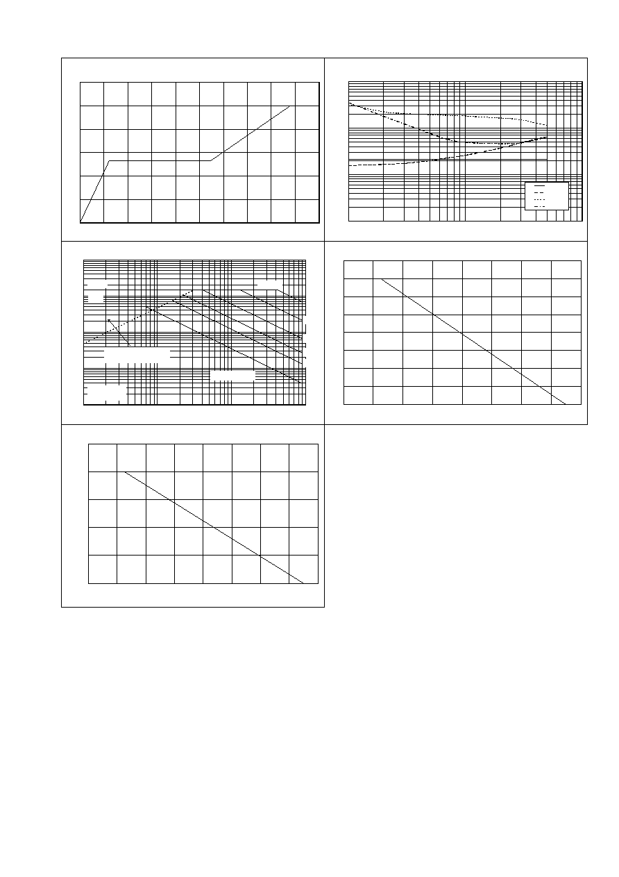
PD - Tc
0
5
10
15
20
25
30
35
40
0
20
40
60
80
100
120
140
160
Case Temperature.Tc-
Allowable Power Dissipation,PD-W