 | –≠–ª–µ–∫—Ç—Ä–æ–Ω–Ω—ã–π –∫–æ–º–ø–æ–Ω–µ–Ω—Ç: LC80101M | –°–∫–∞—á–∞—Ç—å:  PDF PDF  ZIP ZIP |
Overview
The LC80101M is a special-purpose descrambler LSI for
use in VICS systems. FM multiplexed service data that
has had VICS center scrambling applied can be
descrambled and received by inserting this LSI in the
serial interface between the LC72700E and the application
CPU. This architecture also supports reception of regular
transmissions that have not been scrambled. Note that
sample evaluation and product manufacture using this LSI
require a contract with the VICS Center organization.
Functions
∑ VICS scrambled/unscrambled recognition circuit
∑ Dedicated VICS descrambler circuit
∑ CPU interface circuit (CCB: serial)
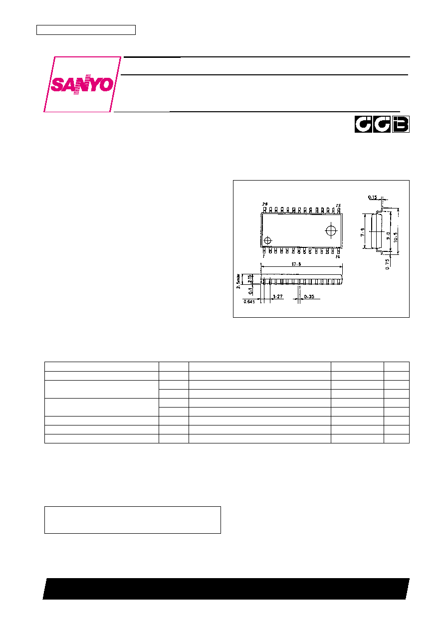
Package Dimensions
unit: mm
3091A-MFP28
CMOS LSI
53096HA (OT) No. 5438-1/9
SANYO: MFP28
[LC80101M]
SANYO Electric Co.,Ltd. Semiconductor Bussiness Headquarters
TOKYO OFFICE Tokyo Bldg., 1-10, 1 Chome, Ueno, Taito-ku, TOKYO, 110 JAPAN
VICS LSI
LC80101M
Ordering number : EN5438
4465
Parameter
Symbol
Conditions
Ratings
Unit
Maximum supply voltage
V
DD
max
V
DD
≠0.3 to +7.0
V
Input voltage
V
IN
1
The CL2, CE2, DI2, RST2, BACKUP, INT-R1, and DI1 pins
≠0.3 to +7.0
V
V
IN
2
Input pins other than V
IN
1
≠0.3 to V
DD
+0.3
V
Output voltage
V
OUT
1
The DO2 pin
≠0.3 to +7.0
V
V
OUT
2
Output pins other than V
OUT
1
≠0.3 to V
DD
+0.3
V
Allowable power dissipation
Pdmax
Ta
85
∞
C
200
mW
Operating temperature
Topr
≠40 to +85
∞
C
Storage temperature
Tstg
≠55 to +125
∞
C
Specifications
Absolute Maximum Ratings
∑ CCB is a trademark of SANYO ELECTRIC CO., LTD.
∑ CCB is SANYO's original bus format and all the bus
addresses are controlled by SANYO.

No. 5438-2/9
LC80101M
Parameter
Symbol
Conditions
Ratings
Unit
min
typ
max
Clock low-level time
t
CL
CL2
0.7
µs
Clock high-level time
t
CH
CL2
0.7
µs
Data setup time
t
SU
CL2, DI2
0.7
µs
Data hold time
t
HD
CL2, DI2
0.7
µs
CE wait time
t
EL
CL2, CE2
0.7
µs
CE setup time
t
ES
CL2, CE2
0.7
µs
CE hold time
t
EH
CL2, CE2
0.7
µs
Data output time
t
DH
DO2: Varies with the value of the pull-up resistor used
1
µs
Serial Input and Output
(See the serial data timing figures.)
Parameter
Symbol
Conditions
Ratings
Unit
min
typ
max
Input high-level voltage
V
IH
CMOS-compatible Schmitt inputs
0.8 V
DD
V
Input low-level voltage
V
IL
Pull-down resistors: INT-R1, TEST1 to TEST4,
0.2 V
DD
V
and TESTON
Input high-level voltage
V
IH
CMOS-compatible Schmitt inputs:
0.8 V
DD
V
Input low-level voltage
V
IL
BACKUP, CE2, CL2, DI1, DI2, and RST2
0.2 V
DD
V
Output high-level voltage
V
OH
I
OH
= ≠4 mA: CE1, CL1, DO1, INT-R2
V
DD
≠ 2.1
V
Output low-level voltage
V
OL
I
OL
= 4 mA: CE1, CL1, DO1, INT-R2
0.4
V
Output low-level voltage
V
OL
I
OL
= 2 mA: DO2
0.4
V
Standby current
Isd
With the BACKUP pin low
0.01
10
µA
Input sensitivity
Vck
Rf = 1 M
, FILCK1 = 3.6 MHz: FILCK1
*
1
1.0
V
DD
Vp-p
Pull-down resistance
Rd
INT-R1, TEST1 to 4, TESTON
70
140
280
k
I
DD
1
Sine wave input: 1 V p-p, V
DD
= 5.0 V
*
2
6
15
mA
Current drain
I
DD
2
Sine wave input: 5 V p-p, V
DD
= 5.0 V
*
2
2.5
7
mA
I
DD
3
Square wave input: 1 V p-p, V
DD
= 5.0 V
*
2
5
13
mA
I
DD
4
Square wave input: 5 V p-p, V
DD
= 5.0 V
*
2
1.5
4
mA
Electrical Characteristics
/Input and Output Levels at Ta = ≠40 to +85∞C, V
DD
= 4.5 to 5.5 V, V
SS
= 0 V
Note 1. Since this LSI operates based on the rising edge of the LC72700E 3.6 MHz output (the FILCK pin), the LC72700E 3.6 MHz output signal must be
input to the FILCK1 pin without inverting the polarity.
2. The current drain varies with the input level and the shape of the clock signal input to the FILCK1 pin. The current drain can be reduced by using
waveforms that are closer to square waves than to sine waves, and by using a signal level that is close to V
DD
. The LC72700E 3.6 MHz output is a
square wave with an output level equal to V
DD
.
Block Diagram
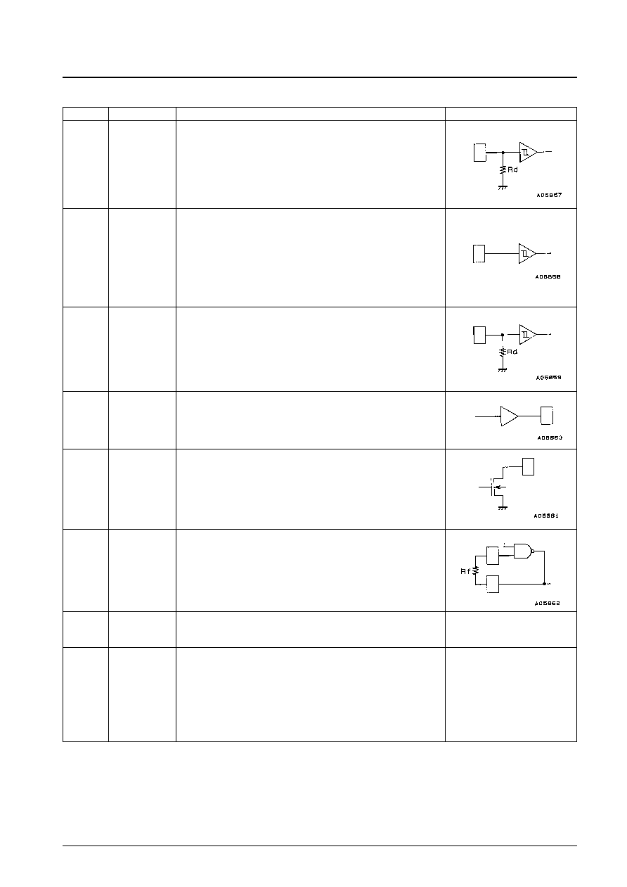
Pin Assignments and Functions
No. 5438-3/9
LC80101M
Pin No.
Pin
Function overview
Input or output circuit type
1
9
19
27
13
TEST1
TEST2
TEST3
TEST4
TESTON
Test pin 1 (Must be connected to ground or left open in normal operation.)
Test pin 2 (Must be connected to ground or left open in normal operation.)
Test pin 3 (Must be connected to ground or left open in normal operation.)
Test pin 4 (Must be connected to ground or left open in normal operation.)
Test pin (Must be connected to ground in normal operation.)
Rd: Input pin internal pull-down resistor
4
INT-R1
Inputs the output of the LC72700E pin 35.
Rd: Input pin internal pull-down resistor
5
20
21
22
23
26
DI1
BACKUP
CL2
CE2
DI2
RST2
Inputs the output of the LC72700E pin 32. An external pull-down resistor is
required. See the following page.
Input that selects normal operation when high and backup mode when low.
Clock input for the CCB serial interface
Control input for the CCB serial interface
Data input for the CCB serial interface
System reset input (negative logic)
6
7
8
25
DO1
CE1
CL1
INT-R2
Output to the LC72700E pin 31 input
Output to the LC72700E pin 30 input
Output to the LC72700E pin 29 input
Outputs an output data interrupt to the external CPU
2
3
FILCK1
FICLK2
System clock generator input
System clock generator output
Rf: External feedback resistor, 510 k
to 1.5 M
(typical: 1 M
)
28
14
V
DD
V
SS
Power supply (+4.5 to 5.5 V)
Ground connection
10, 11,
12, 15,
16, 17
18
NC
No connection pins. These pins must be left open.
24
DO2
Data output for the CCB serial interface
Pin Assignment
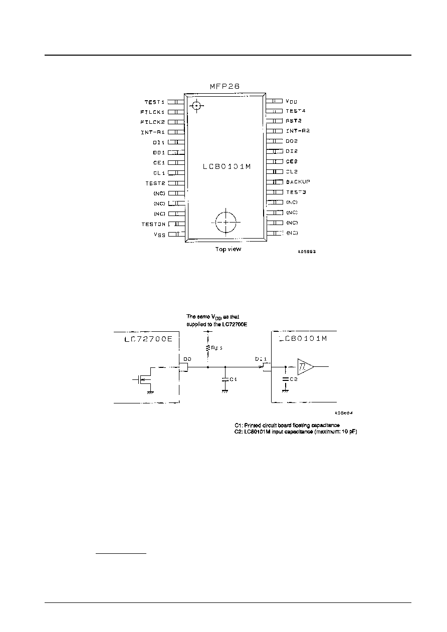
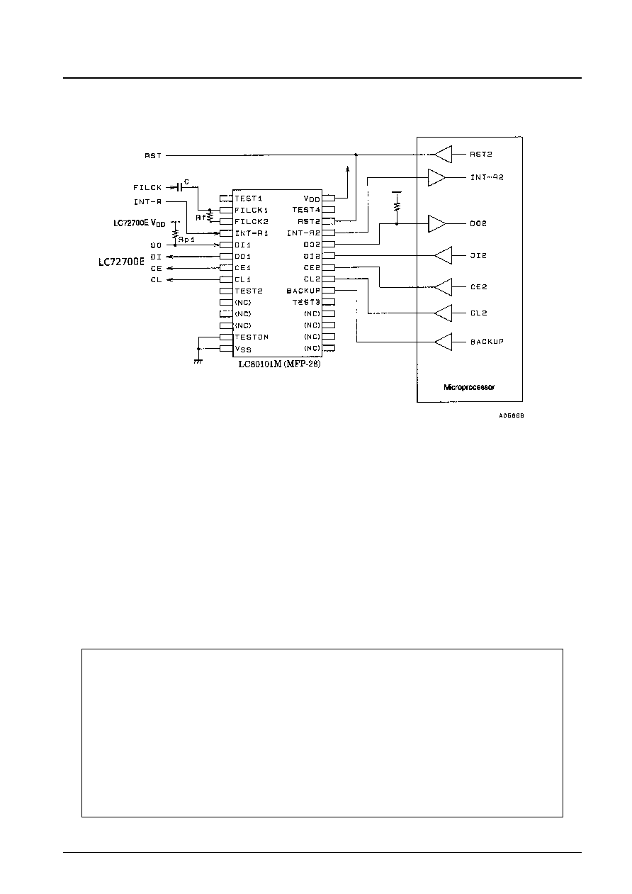
Notes on the pull-up resistor used between the LC72700E pin 32 (DO) and this LSI's pin 5 (DI1)
The value of the pull-up resistor Rp1 must be determined based on the printed circuit board's floating capacitance and the
LC80101M's clock. The time t
CL
for the LC80101M clock is 1.1 µs (corresponding to 450 kHz). This clock is used as
the readout clock output to the LC72700E during the period discussed in note 1 for the basic timing of the external
interface as discussed on page 7. If the t
CL
of the CL2 clock from the microprocessor is longer than the t
CL
of the
LC80101M clock, a t
CL
of 1.1 µs must be used in the formulas below. If the t
CL
of that clock is shorter than that of the
LC80101M clock, then the t
CL
of CL2 must be substituted in the formulas below.
For example, in the configuration shown in the figure above, assuming the t
CL
of CL2 is 1.0 µs (i.e. CL2 = 500 kHz),
then:
T = t
CL
≠ 555 ns (the LC72700E data output time)
Since
T
2.2 (C1 + C2) R
Rp1
Assuming that C1 = 10 pF and C2 = 10 pF, then Rp1 will be
10.1 k
. These considerations must be used as guidelines
when determining the value of the pull-up resistor Rp1.
No. 5438-4/9
LC80101M
445 ns
2.2 (C1 + C2)
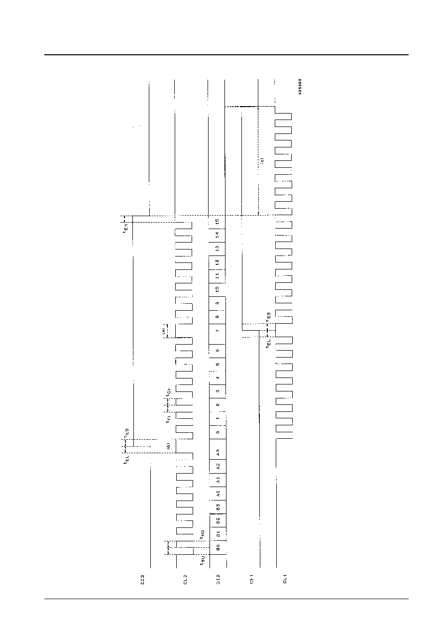
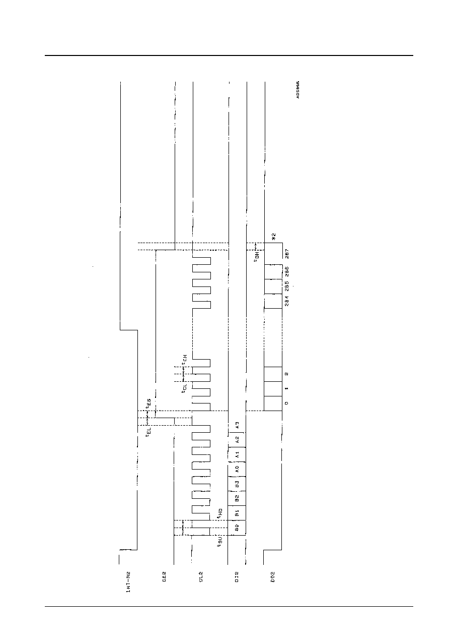
Serial Data Input
No. 5438-5/9
LC80101M
Changes from the serial data input timing in the LC72700E documentation
Since this LSI outputs data to the LC72700E only after receiving and latching 8 bits of data from the microprocessor, it sets C
E1
high during the interval marked (a) in the figure. Therefore it is necessary to create the same periods tEL and tES at (a) as t
hose at
(b). However, it is not necessary to take (a) into consideration if either tHD or tCH is 1.4
µ
s or longer. Note that completion of serial
data input to the LC72700E is the section (c), and this generates a delay 10
µ
s longer than previously. Also, writing and reading
serial data is not allowed during the period (c). (CE2 must be held low during the period (c).)
Note: When an application inputs 16-bit serial control data, if data from the same block is required, the application must fir
st read
out the data from that same block and then input the 16-bit serial control data. If the serial data is input before the data is
read out,
data integrity cannot be guaranteed.
No. 5438-6/9
LC80101M
Serial Data Output
Note:
1.
Since the DO2 pin is an n-channel open-drain pin, the time required for the data value to change differs depending on the
value of the pull-up resistor used.
2.
The DO2 pin is normally open.
Changes from the serial data output timing in the LC72700E documentation
There are no changes related to the CE2, CL2, DI2, and DO2 pins. The trigger signal used by the microprocessor for data
acquisition is the falling edge of either INT-R2 or DO2.
External Interface Basic Timing
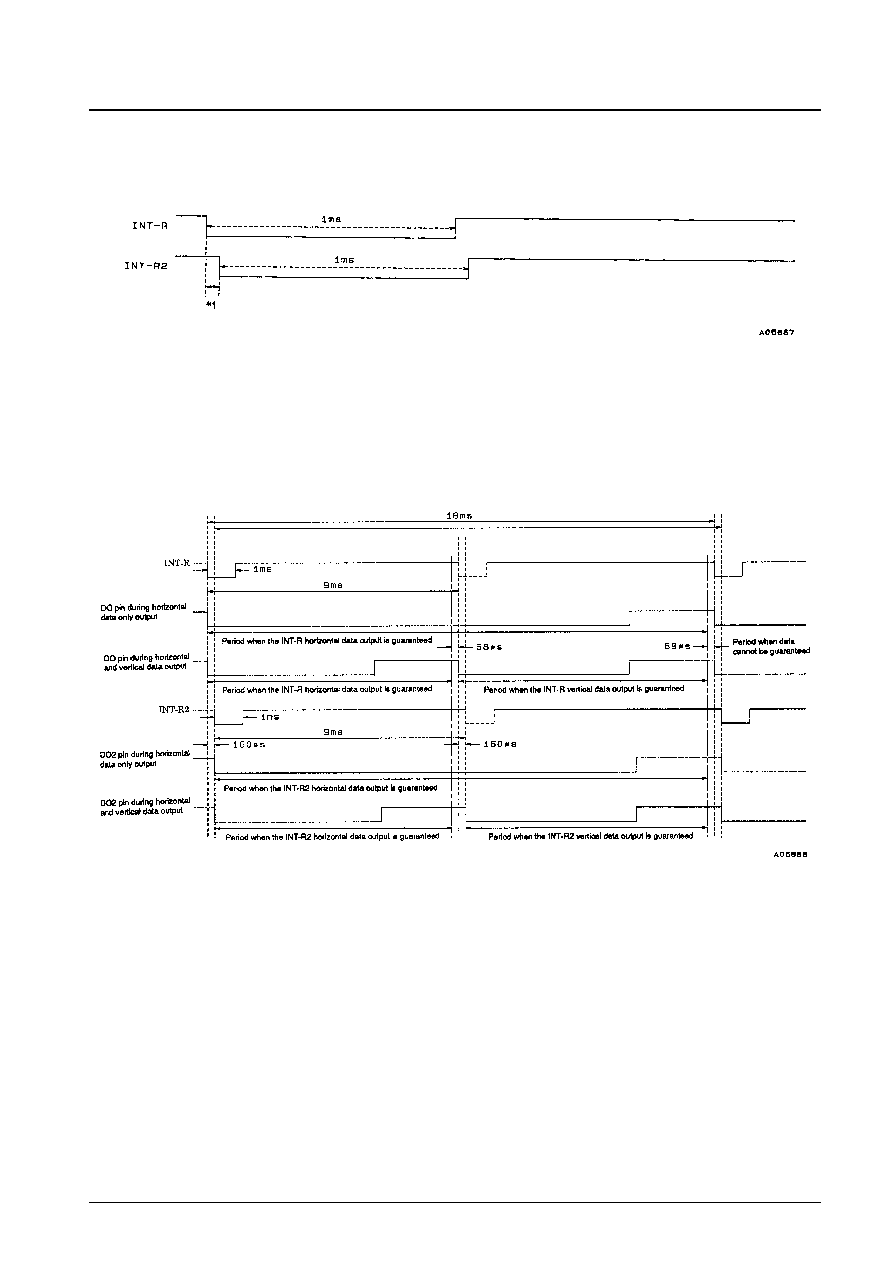
Figure 1
Figure 2
Figure 1 shows how the timing changes between the LC72700E INT-R output and this LSI's INT-R2 output. This LSI
requires the period indicated as "Note 1", about 160 µs, following the detection of a falling edge on the INT-R signal to
set up the descrambling processing. It outputs a falling edge on INT-R2 after the note 1 time has elapsed. Serial data
reads and writes are disabled during this period.
Figure 2 shows the basic timing for the external interface. When this LSI is not used and the system is operated based on
the INT-R trigger, if only horizontal data is output, there will be a data readout guaranteed period of 18 ≠ 0.068 = 17.932
ms, and if both horizontal and vertical data are read out, there will be two 9 ≠ 0.068 = 8.932 ms data readout guaranteed
periods, one each for horizontal and vertical data output. When this LSI is used and the system is operated based on the
INT-R2 trigger, these data readout guaranteed periods are shortened by exactly the amount the INT-R2 signal is delayed,
namely 160 µs. When only horizontal data is output, the data readout guaranteed period will be 17.932 ≠ 0.160 = 17.772
ms, and both horizontal and vertical data is output, the data readout guaranteed periods will be 8.932 ≠ 0.160 = 8.772 ms
for both horizontal and vertical data output.
No. 5438-7/9
LC80101M

Usage Notes
1. Setting the BACKUP pin low switches the LC80101M to backup mode. This is a mode in which oscillator and chip
operation are stopped to reduce current drain. This pin must be set high for normal operation. Also note that a reset
must be applied after the BACKUP pin is returned to high from low. (See Figure 4 on page 8.) The BACKUP pin
must be connected to the LC80101M V
DD
pin if backup mode is not used.
2. The lines connecting this LSI to the LC72700E must be dedicated lines only used by these two chips. Do not connect
these lines to any other circuits via a bus or any other connection.
3. A reset must be applied when power is first applied. The LC72700E RST pin and this LSI's RST2 pin can be driven
from a common signal. (See Figure 3 on page 8.)
4. The TESTON pin (pin 13) must be connected to ground.
Operation During Reset
A reset signal is applied by setting the RST2 pin input level below V
IL
for at least 300 ns when the power-supply voltage
(V
DD
) is 3.4 V or higher. See Figure 3.
Figure 3
All registers other than those holding data required for descrambling are reset by a reset signal. The crystal oscillator
circuit does not stop.
BACKUP Pin
A reset must be applied after the BACKUP pin is returned to high (for normal operation from low (backup mode, in
which the oscillator is stopped). See the following figure.
Figure 4
No. 5438-8/9
LC80101M
PS No. 5438-9/9
LC80101M
Sample Circuit Connecting the LC80101M, the LC72700E, and a Microprocessor
This catalog provides information as of December, 1997. Specifications and information herein are subject to
change without notice.
s
No products described or contained herein are intended for use in surgical implants, life-support systems, aerospace
equipment, nuclear power control systems, vehicles, disaster/crime-prevention equipment and the like, the failure of
which may directly or indirectly cause injury, death or property loss.
s
Anyone purchasing any products described or contained herein for an above-mentioned use shall:
Accept full responsibility and indemnify and defend SANYO ELECTRIC CO., LTD., its affiliates, subsidiaries and
distributors and all their officers and employees, jointly and severally, against any and all claims and litigation and all
damages, cost and expenses associated with such use:
Not impose any responsibility for any fault or negligence which may be cited in any such claim or litigation on
SANYO ELECTRIC CO., LTD., its affiliates, subsidiaries and distributors or any of their officers and employees
jointly or severally.
s
Information (including circuit diagrams and circuit parameters) herein is for example only; it is not guaranteed for
volume production. SANYO believes information herein is accurate and reliable, but no guarantees are made or implied
regarding its use or any infringements of intellectual property rights or other rights of third parties.