
CMOS LSI
Ordering number : EN
*
5218
22896HA (OT) No.5218-1/10
Preliminary
SANYO Electric Co.,Ltd. Semiconductor Bussiness Headquarters
TOKYO OFFICE Tokyo Bldg., 1-10, 1 Chome, Ueno, Taito-ku, TOKYO, 110-8534 JAPAN
1/5" Optical Size CCIR B/W
Solid-State Image Sensor
LC9948G
Overview
The LC9948G is a 1/5" optical size frame transfer type
CCD (charge-coupled device) solid-state image sensor
developed for use in B/W video cameras.
Features
∑ Effective number of pixels (total pixels): 499 H
◊
582 V
(532 H
◊
600 V)
∑ Number of optical black pixels:
Horizontal direction: Front: 7 pixels
Back: 26 pixels
Vertical direction:
Front: 14 pixels
Back: 4 pixels
∑ Dummy bits: Horizontal direction: 4 pixels
∑ Horizontal resolution: 380 TV lines
∑ Supports miniature, compact camera designs.
∑ Package: 20-pin half-pitch transparent DIP
∑ Horizontal shift register: 5 V operation
∑ Supports variable-speed electronic shutter operation
Device Structure
∑ 1/5" type frame transfer CCD image sensor
∑ Unit cell size: 5.8 µm (H)
◊
3.75 µm (V)
∑ Chip size: 4.18 mm (H)
◊
5.10 mm (V)
∑ Parallel gate CCD sensor
∑ Built-in high-sensitivity output amplifier
Specifications
Absolute Maximum Ratings
at Ta = 25∞C, V
SS
= 0 V
Package Dimensions
unit: mm
3217
[LC9948G]
Parameter
Symbol
Conditions
Ratings
Unit
V
DD
V
PW
= 0 V
≠0.3 to +18
V
V
GG
V
PW
= 0 V
≠0.3 to +5
V
Maximum supply voltage
NSUB-PW
≠0.3 to +50
V
NSUB - ¯1 to ¯4,
≠0.3 to +55
V
¯S1 to ¯S4:
Horizontal clock pin
¯R
V
PW
= 0 V
≠0.3 to +18
V
Other clock pins
V
PW
= 0 V
≠15 to +18
V
Other pins
V
PW
= 0 V
≠0.3 to +10
V
Operating temperature
Topr
≠10 to +60
∞C
Storage temperature
Tstg
≠30 to +80
∞C

Specifications
Clock Voltage Conditions
at frame frequency = 3.55 MHz
Note: 1. Insert 47 pF capacitors as shown in Figure 2.
2. Adjust V
HSUB
within the range where image degradation does not occur so that the saturated output level is maximized.
Figure 1
Figure 2
No.5218-4/10
LC9948G
Parameter
Symbol
Conditions
min
typ
max
Unit
Image area clock
Pulse amplitude
V
PIF
*
1
14.0
14.5
15.0
V
¯1, ¯2, ¯3, ¯4
Low level
V
LIF
≠10.0
≠9.5
≠9.0
V
Storage area clock
Pulse amplitude
V
PSL
14.0
14.5
15.0
V
¯S1, ¯S2
Low level
V
LSL
≠7.0
≠6.5
≠6.0
V
Storage area clock
Pulse amplitude
V
PSL
14.0
14.5
15.0
V
¯S3, ¯S4
Low level
V
LSL
≠8.0
≠7.5
≠7.0
V
Horizontal register
Pulse amplitude
V
PH
4.5
5.0
5.5
V
¯H1, ¯H2
Low level
V
LH
0
0
0.5
V
Reset gate clock
Pulse amplitude
V
PR
4.5
5.0
5.5
V
¯R
Low level
V
LR
3.6
4.0
4.4
V
N-Substrate clock
High level
V
HSUB
*
2
See Figure 1
30.0
40.0
V
Low level
V
LSUB
17.5
18.0
18.5
V
Bias Conditions
Note: 1. Design applications so that this level never exceeds the substrate pulse low level V
LSUB
.
2. These are high-impedance inputs.
DC Characteristics
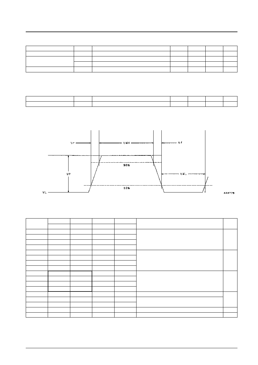
Drive Pulse Waveform Standards
Note:
VP: pulse amplitude
VL: low level
Figure 3 Pulse Waveform
No.5218-5/10
LC9948G
Parameter
Symbol
Conditions
min
typ
max
Unit
P-well
V
PW
0
V
Output circuit voltage
V
DD
*
1
14.5
15.0
15.5
V
V
GG
*
2
0.5
0.8
1.1
V
OG bias
V
OG
*
2
4.5
5.0
5.5
V
Parameter
Symbol
Conditions
min
typ
max
Unit
DC operating current
I
DD
2.5
4.5
6.5
mA
Symbol
t
WH
t
WL
t
r
t
f
Conditions
Unit
typ
typ
typ
typ
¯1
167
102
6.5
6.5
¯2
143
117
11
11
During frame drive
ns
¯3
167
102
6.5
6.5
When the frame shift frequency is 3.55 MHz
¯4
143
117
11
11
¯S1
143
117
11
11
¯S2
143
117
11
11
During frame drive
ns
¯S3
143
117
11
11
When the frame shift frequency is 3.55 MHz
¯S4
143
117
11
11
¯S1
1.4
62.5
30
30
¯S2
1.4
62.5
30
30
The values enclosed in dark lines are in µs units and apply
ns
¯S3
62.5
1.4
30
30
during 1H line transfers.
¯S4
62.5
1.4
30
30
¯R
10
88
4
4
Reset pulse
¯H1
50
50
3
3
During horizontal transfers
ns
¯H2
50
50
3
3
¯NSUB
9.9
19.99
*
0.07
1
Slice pulse
*
value is in ms units.
µs
¯NSUB
4.2
19.99
*
0.07
1
Shutter pulse
*
value is in ms units.
µs

