 | ÐлекÑÑоннÑй компоненÑ: SC1154 | СкаÑаÑÑ:  PDF PDF  ZIP ZIP |
Äîêóìåíòàöèÿ è îïèñàíèÿ www.docs.chipfind.ru
SC1154
PROGRAMMABLE SYNCHRONOUS
DC/DC HYSTERETIC CONTROLLER
FOR ADVANCED PROCESSORS
© 2000 SEMTECH CORP.
652 MITCHELL ROAD NEWBURY PARK CA 91320
PRELIMINARY - March 1, 2000
1
Pentium is a registered trademark of Intel Corporation
TEL:805-498-2111 FAX:805-498-3804 WEB:http://www.semtech.com
DEVICE
(1)
PACKAGE
TEMP. RANGE (T
J
)
SC1154CSW
SO-28
0 - 125°C
ORDERING INFORMATION
Note:
(1) Add suffix `TR' for tape and reel.
DESCRIPTION
The SC1154 is a synchronous-buck switch-mode con-
troller designed for use in single ended power supply
applications where efficiency is the primary concern.
The controller is a hysteretic type, with a user se-
lectable hysteresis. The SC1154 is ideal for imple-
menting DC/DC converters needed to power advanced
microprocessors such as Pentium
®
ll, in both single
and multiple processor configurations. Inhibit, under-
voltage lockout and soft-start functions are included for
controlled power-up.
SC1154 features include an integrated 5 bit D/A con-
verter, temperature compensated voltage reference,
current limit comparator, over-current protection, and
an adaptive deadtime circuit to prevent shoot-through
of the power MOSFET during switching transitions.
Power good signaling, logic compatible shutdown, and
over-voltage protection are also provided. The inte-
grated D/A converter provides programmability of out-
put voltage from 2.0V to 3.5V in 100mV increments
and 1.3V to 2.05V in 50mV increments with no external
components.
The SC1154 high side driver can be configured as ei-
ther a grounded reference or as a floating bootstrap
driver. High and low side drivers have a peak current
rating of 2 amps.
FEATURES
·
Programmable hysteresis
·
5 bit DAC programmable output (1.3V-3.5V)
·
On-chip power good and OVP functions
·
Designed to meet latest Intel specifications
·
Up to 95% efficiency
·
+
1% tolerance over temperature
APPLICATIONS
·
Server Systems and Workstations
·
Pentium
®
II Core Supply
·
Multiple Microprocessor Supplies
·
Voltage Regulator Modules
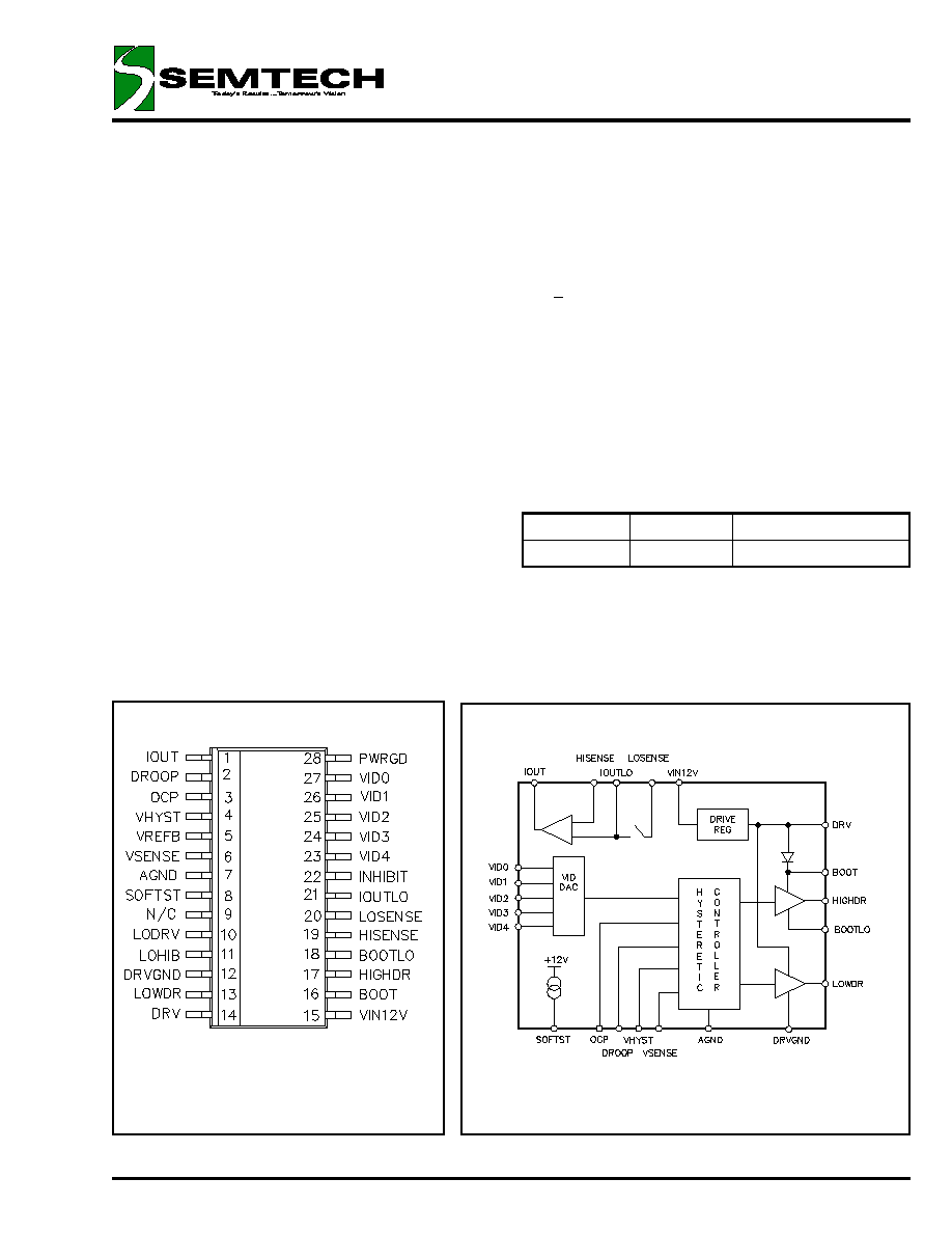
PIN CONFIGURATION
Top View
(28-Pin SOIC)
SIMPLIFIED BLOCK DIAGRAM
SC1154
PROGRAMMABLE SYNCHRONOUS
DC/DC HYSTERETIC CONTROLLER
FOR ADVANCED PROCESSORS
© 2000 SEMTECH CORP.
652 MITCHELL ROAD NEWBURY PARK CA 91320
PRELIMINARY - March 1, 2000
2
ABSOLUTE MAXIMUM RATINGS
Parameter
Symbol
Maximum
Units
VIN12V
VIN
MAX
14
V
BOOT to DRVGND
25
V
BOOT to BOOTLO
15
V
Digital Inputs
-0.3 to +7.3
V
AGND to DRVGND
+
0.5V
V
LOHIB to AGND
14
V
LOSENSE to AGND
14
V
IOUTLO to AGND
14
V
HISENSE to AGND
14
V
VSENSE to AGND
5
V
Continuous Power Dissipation, T
A
= 25°C
P
D
1.2
W
Continuous Power Dissipation, T
C
= 25°C
P
D
6.25
W
Operating Junction Temperature
T
J
0 to +125
°C
Lead Temperature (Soldering) 10 seconds
T
L
300
°C
Storage Temperature
T
STG
-65 to 150
°C
SC1154
PROGRAMMABLE SYNCHRONOUS
DC/DC HYSTERETIC CONTROLLER
FOR ADVANCED PROCESSORS
© 2000 SEMTECH CORP.
652 MITCHELL ROAD NEWBURY PARK CA 91320
PRELIMINARY - March 1, 2000
3
PIN DESCRIPTION
Pin
Pin Name Pin Function
1
IOUT
Current Out. The output voltage on this pin is proportional to the load current as measured
across the high side MOSFET, and is approximately equal to 2 x R
DS(ON)
x I
LOAD
.
2
DROOP
Droop Voltage. This pin is used to set the amount of output voltage set-point droop as a
function of load current. The voltage is set by a resistor divider between IOUT and AGND.
3
OCP
Over Current Protection. This pin is used to set the trip point for over current protection by a
resistor divider between IOUT and AGND.
4
VHYST
Hysteresis Set Pin. This pin is used to set the amount of hysteresis required by a resistor
divider between VREFB and AGND.
5
VREFB
Buffered Reference Voltage (from VID circuitry).
6
VSENSE Output Voltage Sense.
7
AGND
Small Signal Analog and Digital Ground.
8
SOFTST Soft Start. Connecting a capacitor from this pin to AGND sets the time delay.
9
NC
Not connected
10
LODRV
Low Drive Control. Connecting this pin to +5V enables normal operation. When LOHIB is
grounded, this pin can be used to control LOWDR.
11
LOHIB
Low Side Inhibit. This pin is used to eliminate shoot-thru current.
12
DRVGND Power Ground.
13
LOWDR Low Side Driver Output.
14
DRV
Drive Regulator for the MOSFET Drivers.
15
VIN12V
12V Supply.
16
BOOT
Bootstrap. This pin is used to generate a floating drive for the high side FET driver.
17
HIGHDR High Side Driver Output.
18
BOOTLO Bootstrap Low. In desktop applications, this pin connects to DRVGND.
19
HISENSE High Current Sense. Connected to the drain of the high side FET, or the input side of a current
sense resistor between the input and the high side FET.
20
LOSENSE Low Current Sense. Connected to the source of the high side FET, or the FET side of a current
sense resistor between the input and the high side FET.
21
IOUTLO
This is the sampling capacitors bottom leg. Voltage on this pin is voltage on the LOSENSE pin
when the high side FET is on.
22
INHIBIT
Inhibit. If this pin is grounded, the MOSFET drivers are disabled. Usually connected to +5V
through a pull-up resistor.
23
VID4
(1)
Programming Input (MSB).
24
VID3
(1)
Programming Input.
25
VID2
(1)
Programming Input.
26
VID1
(1)
Programming Input.
27
VID0
(1)
Programming Input (LSB).
28
PWRGD
(1)
Power Good. This open collector logic output is high if the output voltage is within 5% of the set
point.
SC1154
PROGRAMMABLE SYNCHRONOUS
DC/DC HYSTERETIC CONTROLLER
FOR ADVANCED PROCESSORS
© 2000 SEMTECH CORP.
652 MITCHELL ROAD NEWBURY PARK CA 91320
PRELIMINARY - March 1, 2000
4
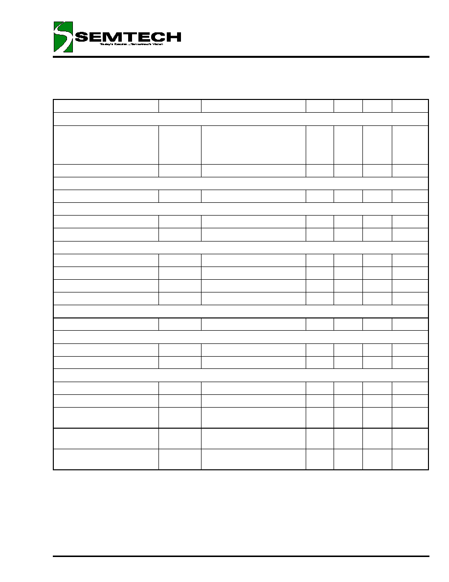
ELECTRICAL CHARACTERISTICS
Unless specified: 0 < T
J
< 125°C, VIN = 12V
PARAMETER
SYMBOL
CONDITIONS
MIN TYP MAX UNITS
Supply Voltage Range
VIN12V
11.4 12
13
V
Supply Current (Quiescent)
I
IN
q
INH = 5V, VID not 11111,
VIN above UVLO threshold during start-up,
f
SW
= 200kHz, BOOTLO = 0V,
C
DH
= C
DL
= 50pF
15
mA
High Side Driver Supply
Current (Quiescent)
I
BOOT
q
INH = 0V or VID = 11111 or VIN below
UVLO threshold during start-up,
BOOT = 13V, BOOTLO = 0V
10
µA
INH = 5V, VID not 11111, VIN
above UVLO threshold during start-up,
f
SW
= 200kHz, BOOT = 13V, BOOTLO = 0V,
C
DH
= 50pF
5
mA
REFERENCE/VOLTAGE IDENTIFICATION
Reference Voltage Accuracy
V
REF
11.4V < VIN12V < 12.6V, over full VID
range (see Output Voltage Table)
-1
1
%
VID0 - VID4 High Threshold
Voltage
V
TH(H)
2.25
V
VID0 - VID4 Low Threshold
Voltage
V
TH(L)
1
V
POWER GOOD
Undervoltage Threshold
V
TH(PWRGD)
90
95
% V
REF
Output Saturation Voltage
V
SAT
I
O
= 5mA
0.5
V
Hysteresis
V
HYS(PWRGD)
10
mV
OVER VOLTAGE PROTECTION
OVP Trip Point
V
OVP
12
15
20
%V
REF
Hysteresis
(1)
V
HYS(OVP)
10
mV
SC1154
PROGRAMMABLE SYNCHRONOUS
DC/DC HYSTERETIC CONTROLLER
FOR ADVANCED PROCESSORS
© 2000 SEMTECH CORP.
652 MITCHELL ROAD NEWBURY PARK CA 91320
PRELIMINARY - March 1, 2000
5
ELECTRICAL CHARACTERISTICS (cont.)
Unless specified: 0 < T
J
< 125°C, VIN = 12V
PARAMETER
SYMBOL
CONDITIONS
MIN
TYP
MAX
UNITS
SOFT START
Charge Current
I
CHG
V
SS
= 0.5V, resistance from
VREFB pin to AGND = 20k
,
V
REFB
= 1.3V
Note: I
CHG
= (I
VREFB
/ 5)
10.4
13
15.6
µA
Discharge Current
Idischg
V
(S/S)
= 1V
1
mA
INHIBIT COMPARATOR
Start Threshold
Vstart
INH
1
2.0
2.4
V
VIN12V UVLO
Start Threshold
Vstart
UVLO
9.25
10
10.75
V
Hysteresis
Vhys
UVLO
1.8
2
2.2
V
HYSTERETIC COMPARATOR
Input Offset Voltage
Vos
HYSCMP
V
DROOP
pin grounded
5
mV
Input Bias Current
Ibias
HYSCMP
1
µA
Hysteresis Accuracy
V
HYS_ACC
7
mV
Hysteresis Setting
V
HYS_SET
60
mV
DROOP COMPENSATION
Initial Accuracy
V
DROOP_ACC
V
DROOP
= 50mV
5
mV
OVERCURRENT PROTECTION
OCP Trip Point
V
OCP
0.09
0.1
0.11
V
Input Bias Current
Ibias
OCP
100
nA
HIGH-SIDE VDS SENSING
Gain
2
V/V
Initial Accuracy
V
IOUT_ACC
V
HISENSE
= 12V, V
IOUTLO
= 11.9V
6
mV
IOUT Source
Isource
IOUT
V
IOUT
= 0.5V, V
HISENSE
= 12V,
V
IOUTLO
= 11.5V
500
µA
IOUT Sink Current
Isink
IOUT
V
IOUT
= 0.05V, V
HISENSE
= 12V,
V
IOUTLO
= 12V
40
50
µA
Output Voltage Swing
V
HISENSE
= 11V,
R
IOUT
= 10k0hm
0
3.75
V