SC1486A data sheet
1
www.semtech.com
SC1486A
Dual Synchronous Buck
DDR and DDR2 Power Supply Controller
POWER MANAGEMENT
Revision: June 22, 2004
Description
Features
Applications
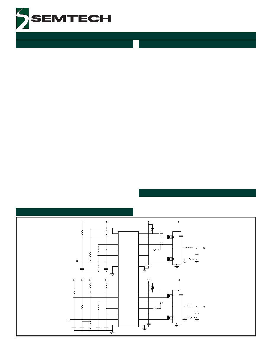
Typical Application Circuit
The SC1486A is a dual output constant on-time
synchronous buck PWM controller optimized for cost
effective mobile DDR and DDR2 applications. Features
include high efficiency, a fast dynamic response with no
minimum on time, a REFIN input and a buffered REFOUT
pin capable of sourcing 3mA. The excellent transient
response means that SC1486A based solutions will
require less output capacitance than competing fixed
frequency converters.
The output voltage of the first controller can be adjusted
from 0.5V to VCCA. In DDR applications, this voltage is
set to 2.5 volts, and in DDR2, 1.8V. A resistor divider
from this supply is used to drive the REFIN pin of the
second controller. A unity gain buffer drives the REFOUT
pin to the same potential as REFIN. The second controller
regulates its output to REFOUT. Two frequency setting
resistors set the on-time for each buck controller. The
frequency can thus be tailored to minimize crosstalk. The
integrated gate drivers feature adaptive shoot-through
protection and soft switching, requiring no gate resistors
for the top MOSFET. Additional features include cycle-
by-cycle current limit, digital soft-start, over-voltage and
under-voltage protection, and a Power Good output for
each controller.
Notebook computers
CPU I/O supplies
Handheld terminals and PDAs
1% DC accuracy
Compatible with DDR & DDR2 memory power
requirements
Constant on-time for fast dynamic response
VIN range = 1.8V � 25V
DC current sense using low-side RDS(ON) sensing
or sense resistor
Integrated reference buffer for VTT
Low power S3 state with high-Z VTT
Resistor programmable on-time
Cycle-by-cycle current limit
Digital soft-start
PSAVE option for VDDQ
Over-voltage/under-voltage fault protection
<20�A shutdown current
Low quiescent power dissipation
Two Power Good indicators
Separate enable for each switcher
Integrated gate drivers with soft switching - no gate
resistors required
Efficiency >90%
28 Lead TSSOP (lead free available)
D1
L1
R1
RTON1
C8
10uF
C13
1uF
C4
1uF
PGOOD
C5
1nF
VTT
VDDQ
C1 0.1uF
VDDQ
5VSUS
5VRUN
VSSA2
VBAT
R5
C2
10uF
C12
100nF
VBAT
Q1
C10
1uF
R6 0R
VDDQ
VSSA2
R8
10k
R9
10R
5VSUS
R3
VSSA1
PGOOD
R7
Q3
VSSA1
VBAT
5VSUS
L2
Q2
Q4
R2
10R
VBAT
+
C3
5VSUS
R14 0R
R10
RTON2
R4
R12
10R
U1
SC1486A
22
23
24
25
26
27
28
1
2
3
4
5
6
7
8
9
10
11
12
13
14
15
16
17
18
19
20
21
EN/PSV1
TON1
VOUT1
VCCA1
FB1
PGD1
VSSA1
PGND1
DL1
VDDP1
ILIM1
LX1
DH1
BST1
REFIN
TON2
REFOUT
VCCA2
FB2
PGD2
VSSA2
PGND2
DL2
VDDP2
ILIM2
LX2
DH2
BST2
VTT
R11
D2
+
C9
C6
1uF
C11
1nF
REFOUT
R15
10k
C7 0.1uF
R13
C14
1uF
2
2004 Semtech Corp.
www.semtech.com
SC1486A
POWER MANAGEMENT
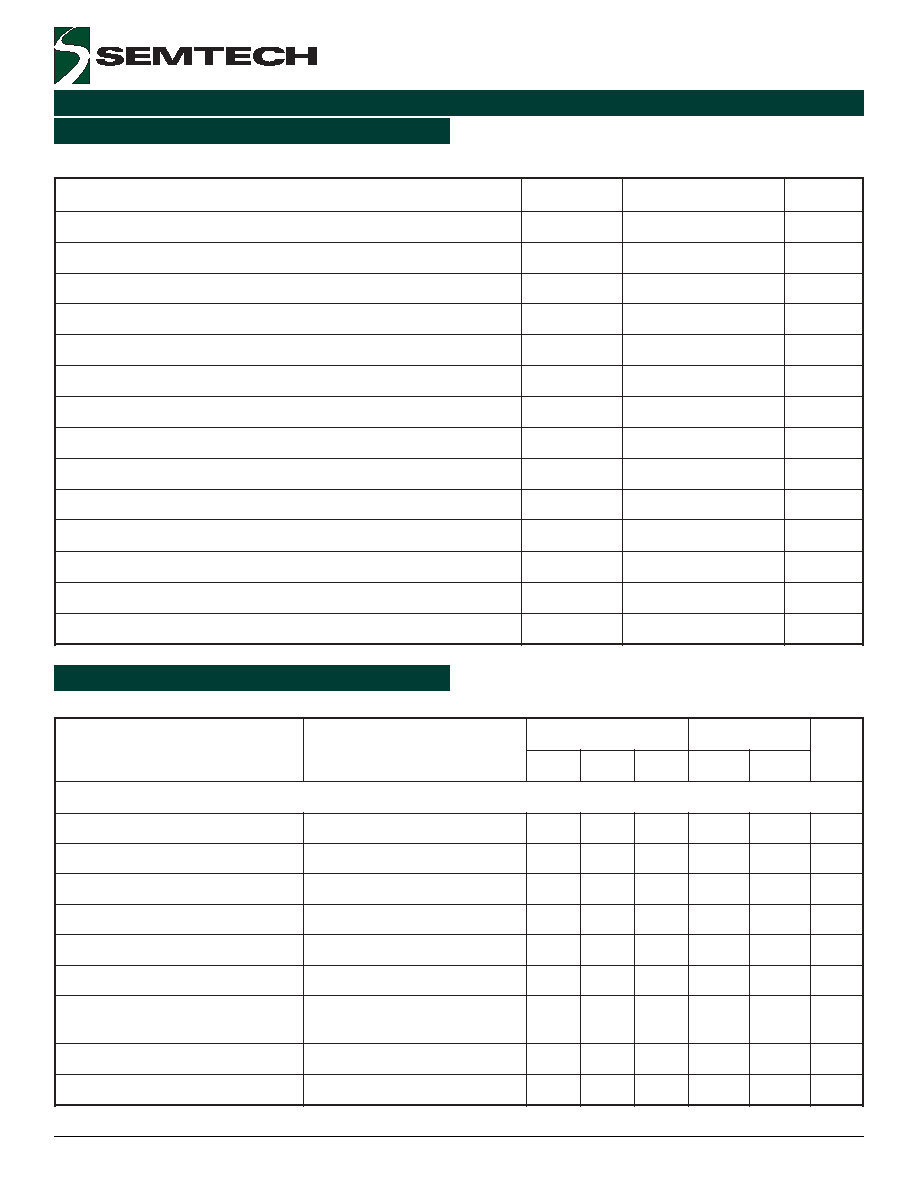
Absolute Maximum Ratings
Electrical Characteristics
Test Conditions: V
BAT
= 15V, EN/PSV1 = 5V, REFIN=1.25V, VCCA1 = VDDP1 = VCCA2 =VDDP2= 5.0V, V
VDDQ
= 2.5, V
VTT
= 1.25, R
TON1
= 1M, R
TON2
= 1M
r
e
t
e
m
a
r
a
P
s
n
o
i
t
i
d
n
o
C
C
�
5
2
C
�
5
2
1
o
t
C
�
0
4
-
s
t
i
n
U
n
i
M
p
y
T
x
a
M
n
i
M
x
a
M
s
e
il
p
p
u
S
t
u
p
n
I
2
A
C
C
V
,
1
A
C
C
V
0
.
5
5
.
4
5
.
5
V
2
P
D
D
V
,
1
P
D
D
V
0
.
5
5
.
4
5
.
5
V
d
l
o
h
s
e
r
h
T
e
g
a
tl
o
v
r
e
d
n
U
2
P
D
D
V
g
n
il
l
a
f
2
P
D
D
V
5
.
3
V
s
i
s
e
r
e
t
s
y
H
e
g
a
tl
o
v
r
e
d
n
U
2
P
D
D
V
0
5
2
V
m
t
n
e
r
r
u
C
g
n
it
a
r
e
p
O
2
P
D
D
V
,
1
P
D
D
V
I
,t
n
i
o
p
n
o
it
a
l
u
g
e
r
>
B
F
D
A
O
L
A
0
=
0
7
0
5
1
A
�
t
n
e
r
r
u
C
g
n
it
a
r
e
p
O
2
A
C
C
V
,
1
A
C
C
V
I
,t
n
i
o
p
n
o
it
a
l
u
g
e
r
>
B
F
D
A
O
L
A
0
=
0
0
7
0
0
1
1
A
�
t
n
e
r
r
u
C
y
b
d
n
a
t
S
2
A
C
C
V
V
U
2
P
D
D
V
<
2
P
D
D
V
T
U
O
F
E
R
n
o
d
a
o
l
o
n
,
d
l
o
h
s
e
r
h
t
5
2
1
A
�
t
n
e
r
r
u
C
g
n
it
a
r
e
p
O
2
N
O
T
,
1
N
O
T
R
N
O
T
M
1
=
5
1
A
�
t
n
e
r
r
u
C
s
a
i
B
N
I
F
E
R
5
2
.
1
=
N
I
F
E
R
1
A
�
Exceeding the specifications below may result in permanent damage to the device, or device malfunction. Operation outside of the parameters
specified in the Electrical Characteristics section is not implied.
r
e
t
e
m
a
r
a
P
l
o
b
m
y
S
m
u
m
i
x
a
M
s
t
i
n
U
2
A
S
S
V
o
t
2
N
O
T
,
1
A
S
S
V
o
t
1
N
O
T
0
.
5
2
+
o
t
3
.
0
-
V
2
D
N
G
P
o
t
2
T
S
B
,
2
H
D
d
n
a
1
D
N
G
P
o
t
1
T
S
B
,
1
H
D
0
.
0
3
+
o
t
3
.
0
-
V
2
D
N
G
P
o
t
2
X
L
d
n
a
1
D
N
G
P
o
t
1
X
L
0
.
5
2
+
o
t
0
.
2
-
V
2
D
N
G
P
o
t
2
A
S
S
V
d
n
a
,
1
D
N
G
P
o
t
1
A
S
S
V
3
.
0
+
o
t
3
.
0
-
V
2
X
L
o
t
2
T
S
B
d
n
a
1
X
L
o
t
1
T
S
B
0
.
6
+
o
t
3
.
0
-
V
2
D
N
G
P
o
t
2
P
D
D
V
,
2
M
I
L
I
,
2
L
D
d
n
a
1
D
N
G
P
o
t
1
P
D
D
V
,
1
M
I
L
I
,
1
L
D
0
.
6
+
o
t
3
.
0
-
V
1
A
S
S
V
o
t
1
T
U
O
V
,
1
A
C
C
V
,
1
D
O
O
G
P
,
1
B
F
,
1
V
S
P
/
N
E
0
.
6
+
o
t
3
.
0
-
V
2
A
S
S
V
o
t
T
U
O
F
E
R
,
N
I
F
E
R
,
2
A
C
C
V
,
2
D
O
O
G
P
,
2
B
F
0
.
6
+
o
t
3
.
0
-
V
1
T
U
O
V
,
1
D
O
O
G
P
,
1
B
F
,
1
V
S
P
/
N
E
o
t
1
A
C
C
V
0
.
6
+
o
t
3
.
0
-
V
T
U
O
F
E
R
,
N
I
F
E
R
,
2
D
O
O
G
P
,
2
B
F
o
t
2
A
C
C
V
0
.
6
+
o
t
3
.
0
-
V
t
n
e
i
b
m
A
o
t
n
o
it
c
n
u
J
e
c
n
a
t
s
i
s
e
R
l
a
m
r
e
h
T
)
5
(
A
J
7
3
W
/
C
�
e
g
n
a
R
e
r
u
t
a
r
e
p
m
e
T
n
o
it
c
n
u
J
g
n
it
a
r
e
p
O
T
J
5
2
1
+
o
t
0
4
-
C
�
e
g
n
a
R
e
r
u
t
a
r
e
p
m
e
T
e
g
a
r
o
t
S
T
G
T
S
0
5
1
+
o
t
5
6
-
C
�
.
c
e
S
0
1
)
g
n
ir
e
d
l
o
S
(
e
r
u
t
a
r
e
p
m
e
T
d
a
e
L
T
D
A
E
L
0
0
3
C
�
3
2004 Semtech Corp.
www.semtech.com
SC1486A
POWER MANAGEMENT
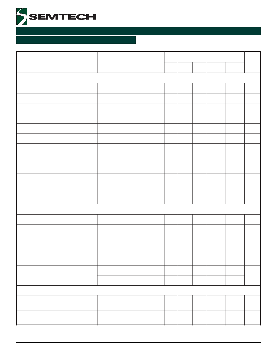
Electrical Characteristics (Cont.)
r
e
t
e
m
a
r
a
P
s
n
o
i
t
i
d
n
o
C
C
�
5
2
C
�
5
2
1
o
t
C
�
0
4
-
s
t
i
n
U
n
i
M
p
y
T
x
a
M
n
i
M
x
a
M
)
.
t
n
o
C
(
s
e
il
p
p
u
S
t
u
p
n
I
t
n
e
r
r
u
C
n
w
o
d
t
u
h
S
V
0
=
1
V
S
P
/
N
E
5
-
0
1
-
A
�
2
A
C
C
V
,
1
A
C
C
V
5
0
1
A
�
1
P
D
D
V
,
2
N
O
T
,
1
N
O
T
0
1
A
�
r
e
ll
o
r
t
n
o
C
d
l
o
h
s
e
r
h
T
r
o
t
a
r
a
p
m
o
C
r
o
r
r
E
)
d
l
o
h
s
e
r
h
T
N
O
n
r
u
T
1
B
F
(
V
5
.
5
o
t
V
5
.
4
=
A
C
C
V
0
0
5
.
0
%
1
-
%
1
+
V
e
g
n
a
R
e
g
a
tl
o
V
t
u
p
t
u
O
Q
D
D
V
5
.
0
A
C
C
V
V
y
ti
li
b
a
p
a
C
e
c
r
u
o
S
T
U
O
F
E
R
3
A
m
y
c
a
r
u
c
c
A
C
D
T
U
O
F
E
R
5
2
.
1
=
N
I
F
E
R
,
d
a
o
l
o
n
4
2
.
1
6
2
.
1
8
3
2
.
1
2
6
2
.
1
V
d
l
o
h
s
e
r
h
T
r
o
t
a
r
a
p
m
o
C
r
o
r
r
E
)
d
l
o
h
s
e
r
h
T
N
O
n
r
u
T
2
B
F
(
V
5
.
5
o
t
V
5
.
4
=
A
C
C
V
T
U
O
F
E
R
T
U
O
F
E
R
V
m
0
1
-
T
U
O
F
E
R
V
m
0
1
+
V
V
5
.
2
=
T
A
B
V
,
e
m
i
T
-
n
O
R
N
O
T
M
1
=
,
V
T
U
O
V
5
2
.
1
=
0
6
6
1
1
1
4
1
9
0
9
1
s
n
R
N
O
T
k
0
0
5
=
,
V
T
U
O
V
5
2
.
1
=
3
1
9
6
7
7
0
5
0
1
s
n
e
m
i
T
ff
O
m
u
m
i
n
i
M
0
0
4
0
5
5
s
n
e
c
n
a
t
s
i
s
e
R
t
u
p
n
I
T
U
O
V
)
r
e
ll
o
r
t
n
o
C
Q
D
D
V
(
0
0
5
k
t
n
e
r
r
u
C
s
a
i
B
t
u
p
n
I
1
B
F
0
.
1
-
0
.
1
+
A
�
t
n
e
r
r
u
C
s
a
i
B
t
u
p
n
I
2
B
F
5
.
2
A
�
g
n
i
s
n
e
S
t
n
e
r
r
u
C
-
r
e
v
O
t
n
e
r
r
u
C
e
c
r
u
o
S
M
I
L
I
h
g
i
H
L
D
0
1
9
1
1
A
�
t
e
s
ff
O
r
o
t
a
r
a
p
m
o
C
t
n
e
r
r
u
C
M
I
L
I
-
D
N
G
P
0
1
-
0
1
+
V
m
E
V
A
S
P
d
l
o
h
s
e
r
h
T
g
n
i
s
s
o
r
C
-
o
r
e
Z
X
L
-
D
N
G
P
V
5
=
1
V
S
P
/
N
E
5
V
m
n
o
i
t
c
e
t
o
r
P
t
l
u
a
F
)
e
v
it
i
s
o
P
(
ti
m
i
L
t
n
e
r
r
u
C
)
2
(
)
X
L
-
D
N
G
P
(
R
M
I
L
I
k
5
=
0
5
5
3
5
6
V
m
R
M
I
L
I
k
0
1
=
0
0
1
0
8
0
2
1
V
m
R
M
I
L
I
k
0
2
=
0
0
2
0
7
1
0
3
2
V
m
)
e
v
it
a
g
e
N
(
ti
m
i
L
t
n
e
r
r
u
C
)
X
L
-
D
N
G
P
(
5
2
1
-
0
6
1
-
0
9
-
V
m
Test Conditions: V
BAT
= 15V, EN/PSV1 = 5V, REFIN=1.25V, VCCA1 = VDDP1 = VCCA2 =VDDP2= 5.0V, V
VDDQ
= 2.5, V
VTT
= 1.25, R
TON1
= 1M, R
TON2
= 1M
4
2004 Semtech Corp.
www.semtech.com
SC1486A
POWER MANAGEMENT
Electrical Characteristics (Cont.)
r
e
t
e
m
a
r
a
P
s
n
o
i
t
i
d
n
o
C
C
�
5
2
C
�
5
2
1
o
t
C
�
0
4
-
s
t
i
n
U
n
i
M
p
y
T
x
a
M
n
i
M
x
a
M
)
.
t
n
o
C
(
n
o
i
t
c
e
t
o
r
P
t
l
u
a
F
tl
u
a
F
e
g
a
tl
o
V
-
r
e
d
n
U
t
u
p
t
u
O
-
Q
D
D
V
.f
e
r
l
a
n
r
e
t
n
i
o
t
t
c
e
p
s
e
r
h
ti
W
0
3
-
0
4
-
5
2
-
%
tl
u
a
F
e
g
a
tl
o
V
-
r
e
d
n
U
t
u
p
t
u
O
-
T
T
V
T
U
O
F
E
R
o
t
t
c
e
p
s
e
r
h
ti
W
0
2
-
8
2
-
5
1
-
%
tl
u
a
F
e
g
a
tl
o
V
-
r
e
v
O
t
u
p
t
u
O
T
T
V
/
Q
D
D
V
l
a
n
r
e
t
n
i
o
t
t
c
e
p
s
e
r
h
ti
w
Q
D
D
V
o
t
t
c
e
p
s
e
r
h
ti
w
T
T
V
,
e
c
n
e
r
e
f
e
r
T
U
O
F
E
R
0
1
+
8
+
2
1
+
%
y
a
l
e
D
tl
u
a
F
e
g
a
tl
o
V
-
r
e
v
O
d
l
o
h
s
e
r
h
t
V
O
e
v
o
b
a
d
e
c
r
o
f
B
F
5
s
�
e
g
a
tl
o
V
t
u
p
t
u
O
w
o
L
D
G
P
A
m
1
k
n
i
S
4
.
0
V
t
n
e
r
r
u
C
e
g
a
k
a
e
L
D
G
P
V
5
=
D
G
P
,
n
o
it
a
l
u
g
e
r
n
i
B
F
1
A
�
d
l
o
h
s
e
r
h
T
V
U
D
G
P
l
a
n
r
e
t
n
i
o
t
t
c
e
p
s
e
r
h
ti
W
d
n
a
Q
D
D
V
r
o
f
e
c
n
e
r
e
f
e
r
T
T
V
r
o
f
T
U
O
F
E
R
0
1
-
5
1
-
8
-
%
y
a
l
e
D
tl
u
a
F
D
G
P
w
o
d
n
i
w
D
G
P
e
d
i
s
t
u
o
d
e
c
r
o
f
B
F
5
s
�
e
g
a
tl
o
V
r
e
d
n
U
2
A
C
C
V
,
1
A
C
C
V
)
s
i
s
e
r
e
t
s
y
h
V
m
0
0
1
(
g
n
il
l
a
F
0
.
4
7
.
3
3
.
4
V
t
u
o
k
c
o
L
e
r
u
t
a
r
e
p
m
e
T
r
e
v
O
s
i
s
e
r
e
t
s
y
H
C
�
0
1
5
6
1
C
�
s
t
u
p
t
u
O
/
s
t
u
p
n
I
e
g
a
tl
o
V
w
o
L
t
u
p
n
I
c
i
g
o
L
w
o
l
1
V
S
P
/
N
E
2
.
1
V
e
g
a
tl
o
V
h
g
i
H
t
u
p
n
I
c
i
g
o
L
)
g
n
it
a
o
l
F
(
w
o
l
V
S
P
,
h
g
i
H
N
E
0
.
2
2
.
1
4
.
2
V
e
g
a
tl
o
V
h
g
i
H
t
u
p
n
I
c
i
g
o
L
h
g
i
h
1
V
S
P
/
N
E
4
.
2
V
d
l
o
h
s
e
r
h
T
N
E
N
I
F
E
R
g
n
i
s
ir
N
I
F
E
R
0
5
.
0
0
6
.
0
V
s
i
s
e
r
e
t
s
y
H
N
E
N
I
F
E
R
0
3
V
m
e
c
n
a
t
s
i
s
e
R
t
u
p
n
I
1
V
S
P
/
N
E
1
A
C
C
V
o
t
p
u
ll
u
p
R
5
.
1
M
1
A
S
S
V
o
t
n
w
o
d
ll
u
p
R
0
.
1
t
r
a
t
S
t
f
o
S
e
m
i
T
p
m
a
R
t
r
a
t
S
-
tf
o
S
,
h
g
i
h
1
D
G
P
o
t
h
g
i
h
1
V
S
P
/
N
E
h
g
i
h
2
D
G
P
o
t
h
g
i
h
N
I
F
E
R
0
4
4
s
k
l
c
)
3
(
e
m
i
T
k
n
a
l
B
e
g
a
tl
o
V
-
r
e
d
n
U
,
h
g
i
h
V
U
o
t
h
g
i
h
1
V
S
P
/
N
E
h
g
i
h
V
U
o
t
h
g
i
h
N
I
F
E
R
0
4
4
s
k
l
c
)
3
(
Test Conditions: V
BAT
= 15V, EN/PSV1 = 5V, REFIN=1.25V, VCCA1 = VDDP1 = VCCA2 =VDDP2= 5.0V, V
VDDQ
= 2.5, V
VTT
= 1.25, R
TON1
= 1M, R
TON2
= 1M
5
2004 Semtech Corp.
www.semtech.com
SC1486A
POWER MANAGEMENT
Notes:
(1) The output voltage will have a DC regulation level higher than the error-comparator threshold by 50% of the
ripple voltage.
(2) Using a current sense resistor, this measurement relates to PGND minus the voltage of the source on the
low-side MOSFET.
(3) clks = switching cycles.
(4) Guaranteed by design. See Shoot-Through Delay Timing Diagram below.
(5) Measured in accordance with JESD51-1, JESD51-2 and JESD51-7.
(6) This device is ESD sensitive. Use of standard ESD handling precautions is required.
Electrical Characteristics (Cont.)
r
e
t
e
m
a
r
a
P
s
n
o
i
t
i
d
n
o
C
C
�
5
2
C
�
5
2
1
o
t
C
�
0
4
-
s
t
i
n
U
n
i
M
p
y
T
x
a
M
n
i
M
x
a
M
s
r
e
v
i
r
D
e
t
a
G
y
a
l
e
D
h
g
u
o
r
h
T
-
t
o
o
h
S
)
4
(
g
n
i
s
ir
L
D
r
o
H
D
0
3
s
n
e
c
n
a
t
s
i
s
e
R
n
w
o
D
-l
l
u
P
L
D
w
o
l
L
D
8
.
0
6
.
1
t
n
e
r
r
u
C
k
n
i
S
L
D
V
5
.
2
=
L
D
1
.
3
e
c
n
a
t
s
i
s
e
R
p
U
-l
l
u
P
L
D
h
g
i
h
L
D
2
4
t
n
e
r
r
u
C
e
c
r
u
o
S
L
D
V
5
.
2
=
L
D
3
.
1
A
e
c
n
a
t
s
i
s
e
R
n
w
o
D
-l
l
u
P
H
D
V
5
=
X
L
-
T
S
B
,
w
o
l
H
D
2
4
e
c
n
a
t
s
i
s
e
R
p
U
-l
l
u
P
H
D
V
5
=
X
L
-
T
S
B
,
h
g
i
h
H
D
2
4
t
n
e
r
r
u
C
e
c
r
u
o
S
/
k
n
i
S
H
D
V
5
.
2
=
L
D
3
.
1
A
Test Conditions: V
BAT
= 15V, EN/PSV1 = 5V, REFIN=1.25V, VCCA1 = VDDP1 = VCCA2 =VDDP2= 5.0V, V
VDDQ
= 2.5, V
VTT
= 1.25, R
TON1
= 1M, R
TON2
= 1M
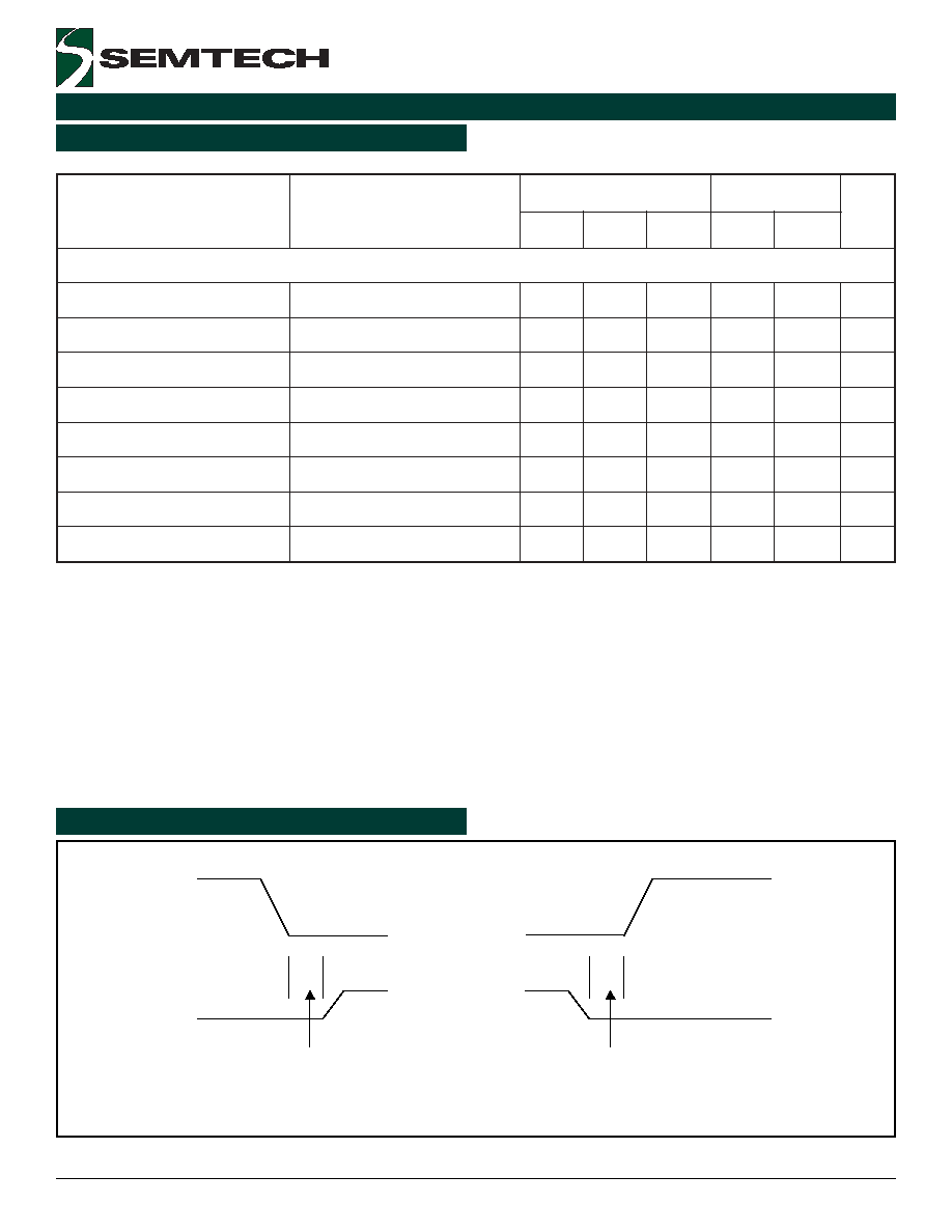
Shoot-Through Delay Timing Diagram
tplhDL
tplhDH
LX
DL
DL
DH