 | ÐлекÑÑоннÑй компоненÑ: SC1543 | СкаÑаÑÑ:  PDF PDF  ZIP ZIP |
Äîêóìåíòàöèÿ è îïèñàíèÿ www.docs.chipfind.ru
© 2000 SEMTECH CORP.
652 MITCHELL ROAD NEWBURY PARK CA 91320
400mA/200mA Dual 3.3V Smart
Power Switch
SC1543
PRELIMINARY - October 9, 2000
1
TEL:805-498-2111 FAX:805-498-3804 WEB:http://www.semtech.com
DESCRIPTION
The SC1543 provides a glitch free 3.3V output when
one of two 3.3V input sources is present. It does not
require external logic to sequence from one input
source to the other. Whenever VIN1 exceeds a
predetermined threshold value the internal MOSFET
connects it's source voltage to the output. If the input at
VIN1 is below the threshold another internal MOSFET
connects VIN2 to the output. If both inputs are at 3.3V
then VIN1 will be connected to the output.
The SC1543 is designed to provide 400mA from the
main input (VIN1) and 200mA from the secondary input
(VIN2). A very low quiescent current of 10µA in
shutdown mode reduces power dissipation.
The internal logic and control circuit detects the voltage
levels of VIN1 and VIN2, and compares them to an
input reference voltage of 2.9V. An internally controlled
period of switch overlap ensures that the transition
between supplies is as glitch-free as possible.
The SC1543 is available in an MSOP-8 surface mount
package.
FEATURES
·
=
Glitch free transitions between inputs
·
=
Internal logic selects appropriate input
·
=
400mA load current capability from main input
·
=
Low power shutdown mode
·
=
Industrial temperature range
APPLICATIONS
·
=
Mini PCI cards
·
=
Peripheral cards
·
=
Instantly available personal computers (IAPCs)
ORDERING INFORMATION
Part Number
(1)
Package
SC1543IMSTR
MSOP-8
Note:
(1) Only available in tape and reel packaging. A reel
contains 2500 devices.
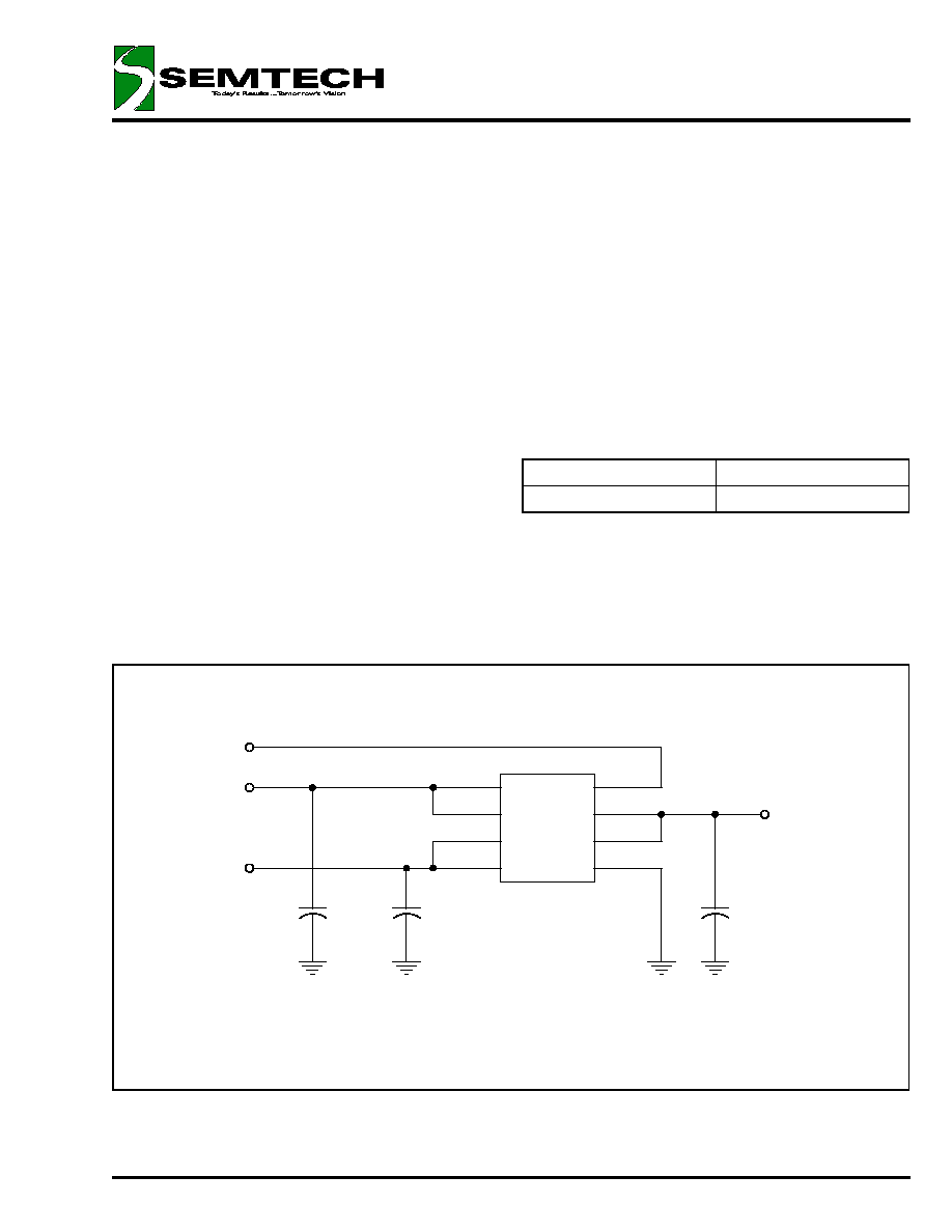
APPLICATION CIRCUIT
3.3V IN
3.3VAUX IN
3.3V OUT
SHUTDOWN
U1
SC1543
1
2
3
4
5
6
7
8
VIN1
VIN1
VIN2
VIN2
GND
VOUT
VOUT
SHDN
COUT
CIN2
CIN1
1uF
1uF
10uF
© 2000 SEMTECH CORP.
652 MITCHELL ROAD NEWBURY PARK CA 91320
400mA/200mA Dual 3.3V Smart
Power Switch
SC1543
PRELIMINARY - October 9, 2000
2
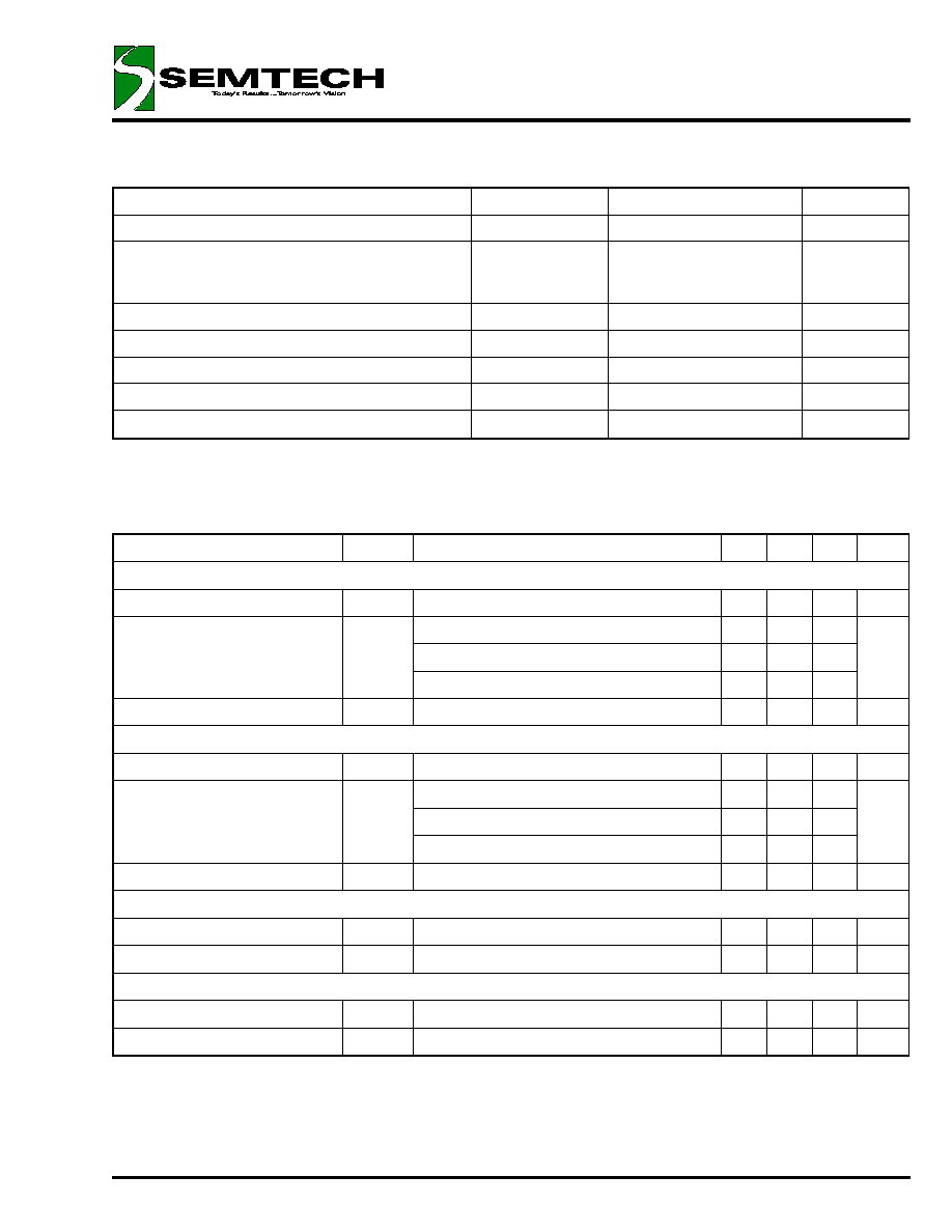
ABSOLUTE MAXIMUM RATINGS
Parameter
Symbol
Maximum
Units
Input Supply Voltage
VIN1,2
-0.5 to +6
V
Output Current From:
VIN1
VIN2
I
O
400
200
mA
Operating Ambient Temperature Range
T
A
-40 to +85
°C
Operating Junction Temperature Range
T
J
-40 to +125
°C
Storage Temperature Range
T
STG
-65 to +150
°C
Lead Temperature (Soldering, 10 Sec.)
T
LEAD
300
°C
Thermal Impedance Junction to Ambient
JA
206
°C/W
ELECTRICAL CHARACTERISTICS
(1)
Unless specified, T
A
= 25°C, SHDN = 0V, C
O
= 10µF, I
O
= 400mA (when power is being supplied from VIN1, 200mA when power is being sup-
plied from VIN2). Values in bold apply over full operating temperature range.
Parameter
Symbol
Conditions
Min
Typ Max Units
VIN1
Supply Voltage
VIN1
3.0
3.3
3.6
V
Quiescent Current
I
Q1
VIN1 > VIN2, I
O
= 0mA
150
300
µA
VIN1 < VIN2
15
50
VIN1 = SHDN = 3.3V
1
10
Reverse Leakage From VIN2
(2)
I
VIN1
VIN1 = 0V, VIN2 = 3.6V, I
O
= 0mA
0.25 1.00
µA
VIN2
Supply Voltage
VIN2
3.0
3.3
3.6
V
Quiescent Current
I
Q2
VIN2 > VIN1, I
O
= 0mA
150
300
µA
VIN2 < VIN1
1
10
VIN2 = SHDN = 3.3V
1
10
Reverse Leakage From VIN1
(2)
I
VIN2
VIN1 = 3.6V, VIN2 = 0V, I
O
= 0mA
0.25 1.00
µA
VIN1 Threshold Voltage
Threshold Voltage
V
TH
2.80 2.90 3.00
V
Hysteresis
V
HYST
130
mV
Power Switches
VIN1 Pass Device R
DS(ON)
(2)
R
DS(ON)1
VIN1 = 3.3V, VIN2 = 0V
100
250
m
VIN2 Pass Device R
DS(ON)
(2)
R
DS(ON)2
VIN1 = 0V, VIN2 = 3.3V
150
400
m
© 2000 SEMTECH CORP.
652 MITCHELL ROAD NEWBURY PARK CA 91320
400mA/200mA Dual 3.3V Smart
Power Switch
SC1543
PRELIMINARY - October 9, 2000
3
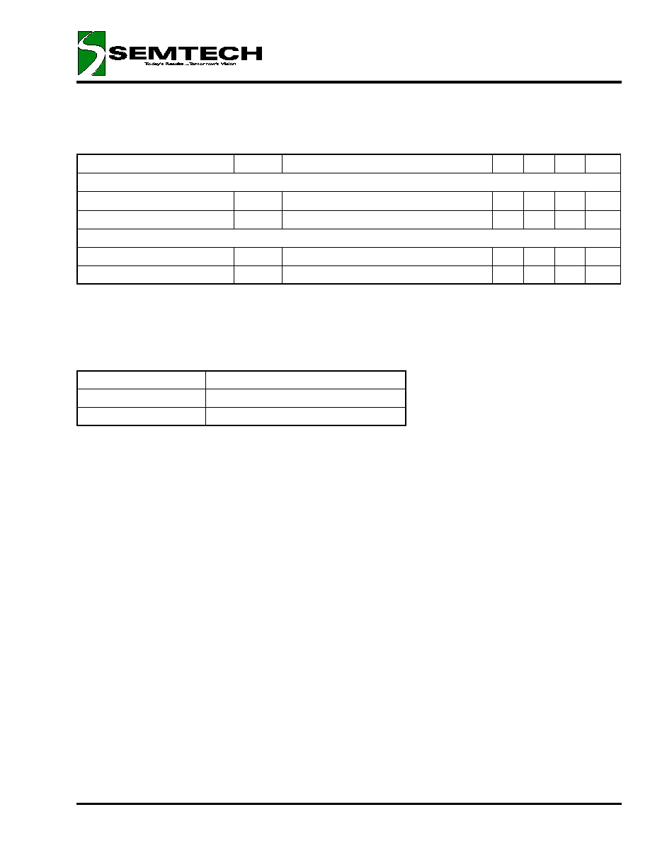
ELECTRICAL CHARACTERISTICS
(1)
(Cont.)
Unless specified, T
A
= 25°C, SHDN = 0V, C
O
= 10µF, I
O
= 400mA (when power is being supplied from VIN1, 200mA when power is being sup-
plied from VIN2). Values in bold apply over full operating temperature range.
Parameter
Symbol
Conditions
Min
Typ Max Units
SHDN
Input High Voltage
V
IH
1.8
V
Input Low Voltage
V
IL
0.4
V
Over Temperature Protection
High Trip Level
T
HI
165
°C
Hysteresis
T
HYS
20
°C
NOTES:
(1) This device is ESD sensitive. Use of standard ESD handling precautions is required.
(2) Guaranteed by design.
OUTPUT TRUTH TABLE
NOTES:
(1) See Electrical Characteristics for definition for V
TH
.
Input Conditions
(1)
VOUT
VIN1 > V
TH
Connected to VIN1
VIN1 < V
TH
Connected to greater of VIN1 and VIN2
© 2000 SEMTECH CORP.
652 MITCHELL ROAD NEWBURY PARK CA 91320
400mA/200mA Dual 3.3V Smart
Power Switch
SC1543
PRELIMINARY - October 9, 2000
4
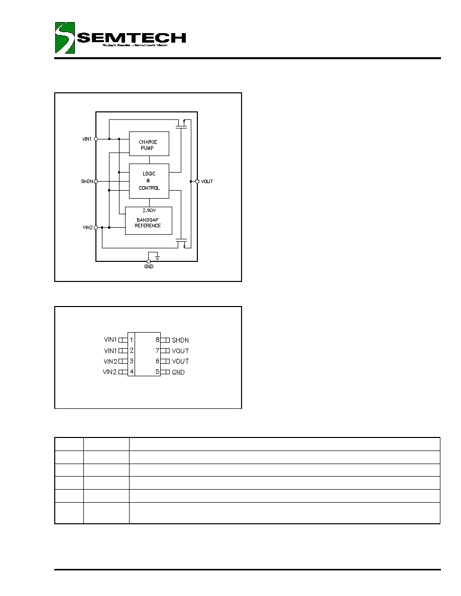
PIN CONFIGURATION
(MSOP-8)
Top View
BLOCK DIAGRAM
PIN DESCRIPTION
Pin
Pin Name
Pin Function
1,2
VIN1
Primary input supply, nominally 3.3V.
3,4
VIN2
Secondary input supply, nominally 3.3V.
5
GND
Power and logic ground.
6,7
VOUT
3.3V out.
8
SHDN
Shutdown, with internal pull-down. Device is OFF when this pin is High. Leave open if shut-
down feature is not required.
© 2000 SEMTECH CORP.
652 MITCHELL ROAD NEWBURY PARK CA 91320
400mA/200mA Dual 3.3V Smart
Power Switch
SC1543
PRELIMINARY - October 9, 2000
5
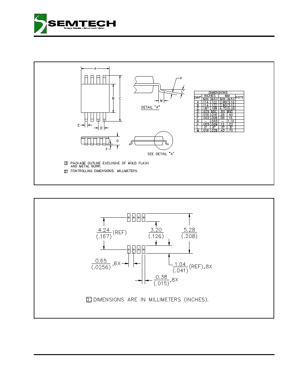
OUTLINE DRAWING - MSOP-8
LAND PATTERN - MSOP-8
ECN00-1361