
PRELIMINARY
1
www.semtech.com
PROTECTION PRODUCTS
SLVU2.8-8
EPD TVSTM
TM
TM
TM
TM Diode Array
For ESD and Latch-Up Protection
Description
Features
Circuit Diagram (Each Line)
Schematic & PIN Configuration
Revision 08/21/2002
The SLV series of transient voltage suppressors are
designed to protect low voltage, state-of-the-art CMOS
semiconductors from transients caused by electro-
static discharge (ESD), cable discharge events (CDE),
lightning and other induced voltage surges.
The devices are constructed using Semtech's propri-
etary EPD process technology. The EPD process pro-
vides low standoff voltages with significant reductions
in leakage currents and capacitance over silicon-
avalanche diode processes. The SLVU2.8-8 features
integrated low capacitance compensation diodes that
reduce the maximum capacitance to 8pF per line.
This, combined with low leakage current, means signal
integrity is preserved in high-speed applications such
as 10/100/1000 Ethernet.
The SLVU2.8-8 is in an SO-8 package and may be used
to protect four high-speed line pairs. The layout of the
device minimizes trace inductance and reduces voltage
overshoot associated with ESD events. The low
clamping voltage of the SLVU2.8-8 minimizes the
stress on the protected IC.
The SLV series TVS diodes will meet the surge require-
ments of IEC 61000-4-2 (ESD), IEC61000-4-5 (Light-
ning), and ETSI ETS 300 386.
Applications
Mechanical Characteristics
10/100/1000 Ethernet
WAN/LAN Equipment
Switching Systems
DSLAMs
Desktops, Servers, & Notebooks
Instrumentation
Base Stations
Analog Inputs
600 Watts peak pulse power (tp = 8/20�s)
Transient protection for high speed data lines to
IEC 61000-4-2 (ESD) 15kV (air), 8kV (contact)
IEC 61000-4-4 (EFT) 40A (tp = 5/50ns)
IEC 61000-4-5 (Lightning) 24A (tp = 8/20�s)
Protects four line pairs (eight lines)
Comprehensive pin out for easy board layout
Low capacitance
High peak pulse current (30A, 8/20�s)
Low leakage current
Low operating and clamping voltages
Solid-state EPD TVS process technology
JEDEC SO-8 package
Molding compound flammability rating: UL 94V-0
Marking : Part number, date code, logo
Packaging : Tape and Reel per EIA 481
SO-8 (Top View)

2
2002 Semtech Corp.
www.semtech.com
PROTECTION PRODUCTS
SLVU2.8-8
Absolute Maximum Rating
Electrical Characteristics (T=25
o
C)
g
n
i
t
a
R
l
o
b
m
y
S
e
u
l
a
V
s
t
i
n
U
0
2
/
8
=
p
t
(
r
e
w
o
P
e
s
l
u
P
k
a
e
P
� )
s
P
k
p
0
0
6
s
t
t
a
W
0
2
/
8
=
p
t
(
t
n
e
r
r
u
C
e
s
l
u
P
k
a
e
P
� )
s
I
P
P
0
3
A
)
r
i
A
(
2
-
4
-
0
0
0
1
6
C
E
I
r
e
p
D
S
E
)
t
c
a
t
n
o
C
(
2
-
4
-
0
0
0
1
6
C
E
I
r
e
p
D
S
E
V
D
S
E
0
3
5
2
V
k
e
r
u
t
a
r
e
p
m
e
T
g
n
ir
e
d
l
o
S
d
a
e
L
T
L
)
s
d
n
o
c
e
s
0
1
(
0
4
2
o
C
e
r
u
t
a
r
e
p
m
e
T
g
n
it
a
r
e
p
O
T
J
5
2
1
+
o
t
5
5
-
o
C
e
r
u
t
a
r
e
p
m
e
T
e
g
a
r
o
t
S
T
G
T
S
0
5
1
+
o
t
5
5
-
o
C
8
-
8
.
2
U
V
L
S
r
e
t
e
m
a
r
a
P
l
o
b
m
y
S
s
n
o
i
t
i
d
n
o
C
m
u
m
i
n
i
M
l
a
c
i
p
y
T
m
u
m
i
x
a
M
s
t
i
n
U
e
g
a
tl
o
V
f
f
O
-
d
n
a
t
S
e
s
r
e
v
e
R
V
M
W
R
8
.
2
V
e
g
a
tl
o
V
h
g
u
o
r
h
T
-
h
c
n
u
P
V
T
P
I
T
P
A
�
2
=
0
.
3
V
e
g
a
tl
o
V
k
c
a
B
-
p
a
n
S
V
B
S
I
B
S
A
m
0
5
=
8
.
2
V
t
n
e
r
r
u
C
e
g
a
k
a
e
L
e
s
r
e
v
e
R
I
R
V
M
W
R
C
�
5
2
=
T
,
V
8
.
2
=
)
e
n
i
L
h
c
a
E
(
0
0
1
.
1
A
�
e
g
a
tl
o
V
g
n
i
p
m
a
l
C
V
C
I
P
P
s
�
0
2
/
8
=
p
t
,
A
1
=
)
e
n
i
L
h
c
a
E
(
6
.
4
V
e
g
a
tl
o
V
g
n
i
p
m
a
l
C
V
C
I
P
P
s
�
0
2
/
8
=
p
t
,
A
4
2
=
)
e
n
i
L
h
c
a
E
(
5
1
V
e
g
a
tl
o
V
g
n
i
p
m
a
l
C
V
C
I
P
P
s
�
0
2
/
8
=
p
t
,
A
0
3
=
)
e
n
i
L
h
c
a
E
(
7
1
V
t
n
e
r
r
u
C
e
s
l
u
P
k
a
e
P
m
u
m
i
x
a
M
I
P
P
s
�
0
2
/
8
=
p
t
0
3
A
e
c
n
a
ti
c
a
p
a
C
n
o
it
c
n
u
J
C
j
V
R
z
H
M
1
=
f
,
V
0
=
)
e
n
i
L
h
c
a
E
(
8
F
p
3
2002 Semtech Corp.
www.semtech.com
PROTECTION PRODUCTS
PRELIMINARY
PROTECTION PRODUCTS
SLVU2.8-8
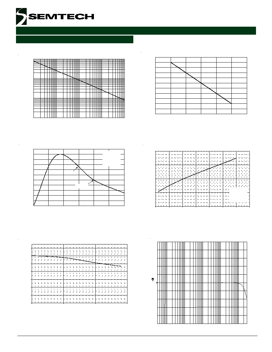
Typical Characteristics
Non-Repetitive Peak Pulse Power vs. Pulse Time
0
10
20
30
40
50
60
70
80
90
100
110
0
25
50
75
100
125
150
Ambient Temperature - T
A
(
o
C)
% of Rated Power or I
PP
Power Derating Curve
Pulse Waveform
Clamping Voltage vs. Peak Pulse Current
0
10
20
30
40
50
60
70
80
90
100
110
0
5
10
15
20
25
30
Time (
�
�
�
�s)
Percent of I
PP
e
-t
td = I
PP
/2
Waveform
Parameters:
tr = 8
�s
td = 20
�s
Capacitance vs. Reverse Voltage
0
4
8
12
16
0
5
10
15
20
25
30
35
Peak Pulse Current Ipp - (A)
Clamping Voltage Vc - (V
)
Waveform
Parameters:
tr = 8
�s
td = 20
�s
0.01
0.1
1
10
0.1
1
10
100
1000
Pulse Duration - tp (
�
�
�
�s)
Peak Pulse Power - P
PP
(kW)
6
6.2
6.4
6.6
6.8
7
7.2
7.4
0
1
2
3
Bias Voltage (V)
Capacitance (pF)
CH1
S21 LOG
10 dB/
REF 0 dB
START
.030 000 MHz
STOP 3 000. 000 000 MHz
Insertion Loss S21
4
2002 Semtech Corp.
www.semtech.com
PROTECTION PRODUCTS
SLVU2.8-8
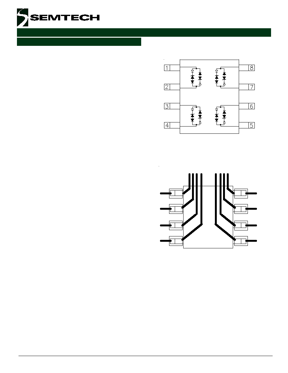
SLVU2.8-8 Circuit Diagram
Differential Protection of Four Line Pairs
Device Connection for Protection of Eight Data Lines
Electronic equipment is susceptible to transient distur-
bances from a variety of sources including: ESD to an
open connector or interface, direct or nearby lightning
strikes to cables and wires, and charged cables "hot
plugged" into I/O ports. The SLVU2.8-8 is designed to
protect sensitive components from damage and latch-
up which may result from such transient events. The
SLVU2.8-8 can be configured to protect four high-
speed line pairs differentially, or four lines to ground
(common mode). The device is connected as follows:
1. Differential Protection of four line pairs:
Line pairs are connected at pins 1 and 2, 3 and 4,
5 and 6, and 7 and 8.
Circuit Board Layout Recommendations for Suppres-
sion of ESD.
Good circuit board layout is critical for the suppression
of ESD induced transients. The following guidelines are
recommended:
Place the device near the input terminals or con-
nectors to restrict transient coupling.
Minimize the path length between the TVS and the
protected line.
Minimize all conductive loops including power and
ground loops.
The ESD transient return path to ground should be
kept as short as possible.
Never run critical signals near board edges.
Use ground planes whenever possible.
Applications Information
1
2
3
4
5
6
7
8
From Connector
5
2002 Semtech Corp.
www.semtech.com
PROTECTION PRODUCTS
PRELIMINARY
PROTECTION PRODUCTS
SLVU2.8-8
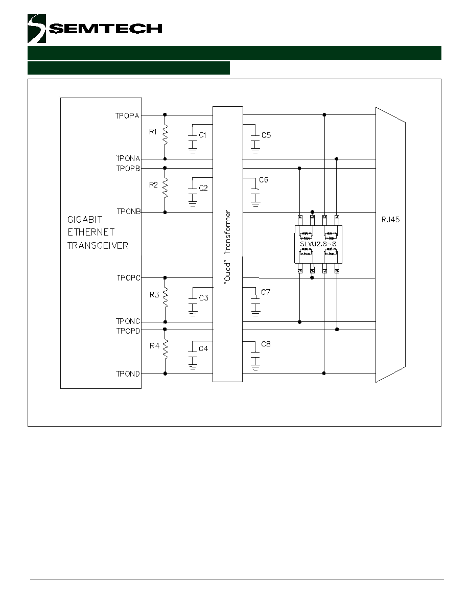
Gigabit Ethernet Protection Circuit
Typical Applications

6
2002 Semtech Corp.
www.semtech.com
PROTECTION PRODUCTS
SLVU2.8-8
Typical Applications
One SLVU2.8.8 Protecting Two 10/100 Ethernet Port
7
2002 Semtech Corp.
www.semtech.com
PROTECTION PRODUCTS
PRELIMINARY
PROTECTION PRODUCTS
SLVU2.8-8
Applications Information (continued)
I
P P
I
SB
I
PT
I
R
V
RWM
V
V
PT
V
C
V
BRR
I
BRR
SB
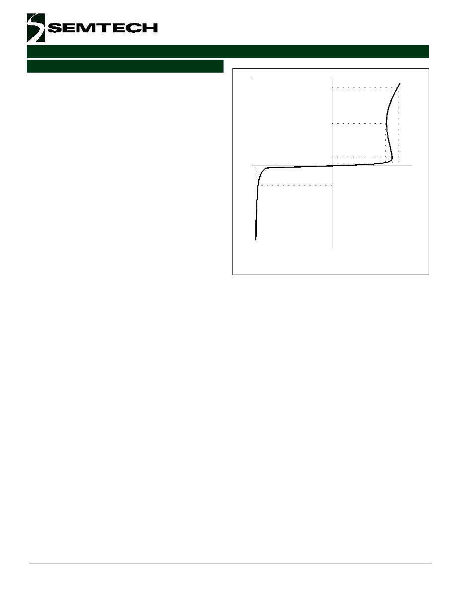
EPD TVS VI Characteristic Curve
EPD TVSTM Characteristics
The SLVU2.8-8 is constructed using Semtech's propri-
etary EPD technology. The structure of the EPD TVS is
vastly different from the traditional pn-junction devices.
At voltages below 5V, high leakage current and junction
capacitance render conventional avalanche technology
impractical for most applications. However, by utilizing
the EPD technology, the SLVU2.8-8 can effectively
operate at 2.8V while maintaining excellent electrical
characteristics.
The EPD TVS employs a complex nppn structure in
contrast to the pn structure normally found in tradi-
tional silicon-avalanche TVS diodes. The EPD mecha-
nism is achieved by engineering the center region of
the device such that the reverse biased junction does
not avalanche, but will "punch-through" to a conduct-
ing state. This structure results in a device with supe-
rior dc electrical parameters at low voltages while
maintaining the capability to absorb high transient
currents.
The IV characteristic curve of the EPD device is shown
in Figure 1. The device represents a high impedance
to the circuit up to the working voltage (V
RWM
). During a
transient event, the device will begin to conduct as it is
biased in the reverse direction. When the punch-
through voltage (V
PT
) is exceeded, the device enters a
low impedance state, diverting the transient current
away from the protected circuit. When the device is
conducting current, it will exhibit a slight "snap-back" or
negative resistance characteristic due to its structure.
This must be considered when connecting the device
to a power supply rail. To return to a non-conducting
state, the current through the device must fall below
the snap-back current (approximately < 50mA).

8
2002 Semtech Corp.
www.semtech.com
PROTECTION PRODUCTS
SLVU2.8-8
Land Pattern - SO-8
Outline Drawing - SO-8

9
2002 Semtech Corp.
www.semtech.com
PROTECTION PRODUCTS
PRELIMINARY
PROTECTION PRODUCTS
SLVU2.8-8
Contact Information
Semtech Corporation
Protection Products Division
200 Flynn Road, Camarillo, CA 93012
Phone: (805)498-2111 FAX (805)498-3804
Ordering Information
r
e
b
m
u
N
t
r
a
P
g
n
i
k
r
o
W
e
g
a
t
l
o
V
l
e
e
R
r
e
p
y
t
Q
e
z
i
S
l
e
e
R
B
T
.
8
-
8
.
2
U
V
L
S
V
8
.
2
0
0
5
h
c
n
I
7
E
T
.
8
-
8
.
2
U
V
L
S
V
8
.
2
0
0
5
,
2
h
c
n
I
3
1
Note:
(1) No suffix indicates tube pack.
SC YYWW
SLVU2.8
-8
1
Marking
Note:
(1) yyww = Date Code
Top View