
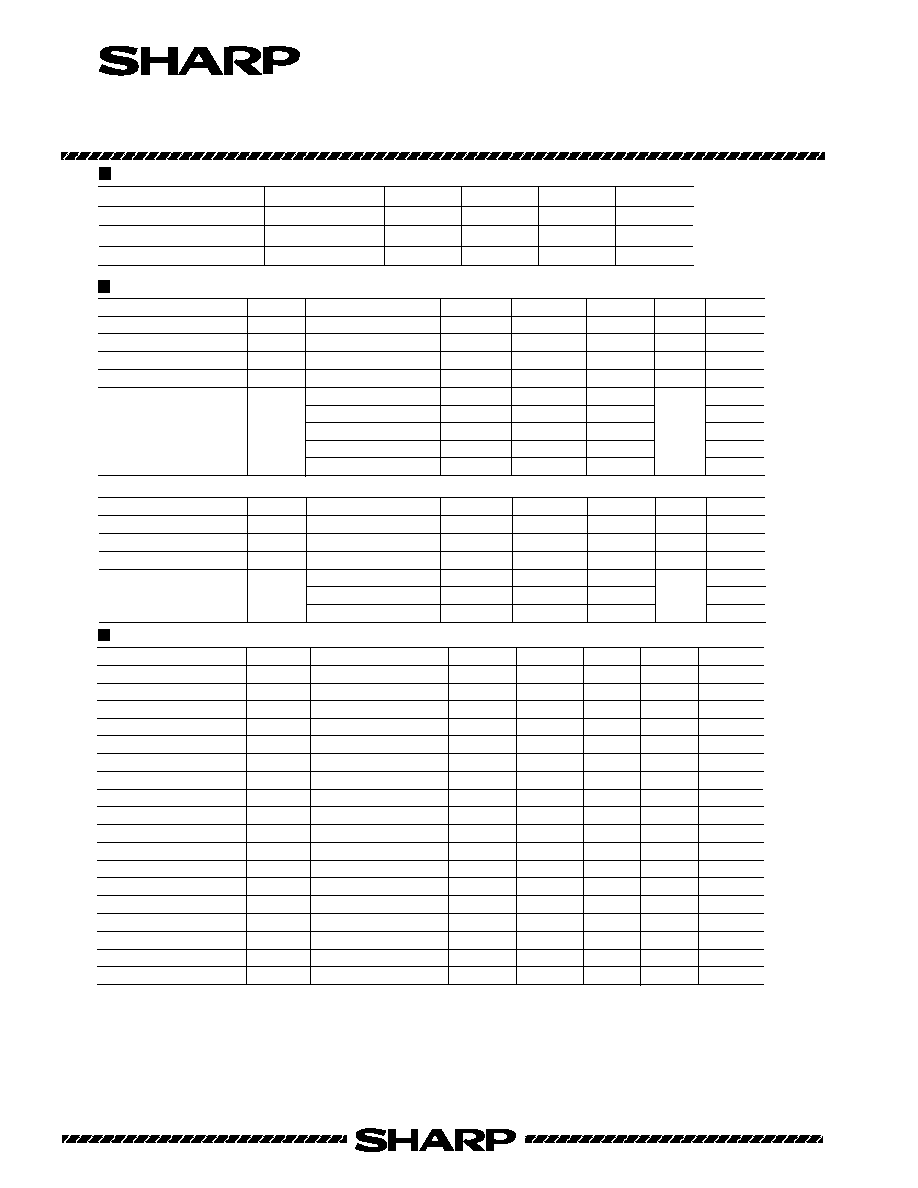
(Unit: mm)
IS1682
Tec.IS980701
General Description
Outline Dimensions
Features
Applications
Absolute Maximum Ratings
OPIC Light Detector
OPIC Light Detector for X40 Speed CD-ROM Drive
Sharp's
IS1682
is OPIC light detectors which
are used for pick-up in X40 speed CD-ROM drive.
They improve noise resistance characteristics and
enable to read low reflective CD-RW due to built-in
RF amp.
(1) High speed response(Response frequency: MIN. 45MHz)
(Best suited for optical pick-up in X40 speed CD-ROM drive)
(2) With built-in RF amplifier
(Integrates 6-division PIN photodiode and
amplifier circuit onto a single chip)
(3) Compact and thin package
(Dimensions: 5.0 x 4.0 x 1.5mm)
(4) Possible to supply custom-made detecting pattern
(5) Pair use with Sharp's laser diode is recommended.
Laser diode : 780 nm / 5 mW (LT022 series )
770 to 795 nm /60 mW ( LT041NS )
(1) CD-ROM drive(to 40X speed)
(2) CD-ROM drive for CD-RW
* "OPIC"(Optical IC)is a trademark of the SHARP Corporation. An OPIC consists of a
light-detecting element and signal-processing circuit integrated ontoa single chip.
(Ta=25∞C)
Parameter Symbol Rating Unit
Supply voltage Vcc 6.0 V
*1 Output voltage Vo Vcc V
Operating temperature Topr
-
30 to +80 ∞C
Storage temperature Tstg
-
40 to +100 ∞C
Soldering temperature Tsol 260
∞C
*1 Applies to V
A
to V
F,
V
RF
*2 For MAX.3s at the position of 1.0mm from the resin edge.
1
2
3
4
5
6
7
8
9
10
V
F
V
RF
V
B
V
E
V
S
Vcc
V
D
V
C
V
A
GND
Terminal connection
5
6
7
8
9
10
(2.2)
2.0
0.35
0.4
P=0.8
4.0
0.15
5.0
1.5
8.4
4
3
2
1
Under development
New product
*2
380
A B
C
D
4-15
4-15
E
F
66
200
120
88
66 124
124
Unit:
µ
m
6∞
6∞
5
5
Detecting Pattern of Photodiode
-
+
Bias circuit
-
+
-
+
E
F
-
+
-
+
-
+
-
+
Vcc
A
B
C
D
GND
V
RF
V
F
V
E
V
D
V
C
V
B
V
A
V
S
Internal Block Diagram
(Notice)
(Internet)
∑ Data for Sharp's optoelectronic/power devices is provided on internet. ( Address http://www.sharp.co.jp/ecg/)
∑ In the absence of confirmation by device specification sheets, SHARP takes no responsibility for any defects that may occur in equipment using
any SHARP devices shown in catalogs, data books, etc. Contact SHARP in order to obtain the latest device specification sheets before using any
SHARP device.
∑ Specifications are subject to change without notice for improvement.
IS1682
OPIC Light Detector
Tec.IS980701
Recommended Operating Conditions
Electrical Characteristics 1
(Ta=25∞C)
Parameter
Symbol
MIN.
TYP.
MAX.
Unit
Operating supply voltage
Vcc
4.75
5.0
5.25
V
Operating supply voltage 1
Vs
2.0
2.1
2.2
V
(Ta=25∞C,Vcc=5V,Vs=2.1V,R
L
=10k
[ V
RF
terminal : R
L
= 0
] C
L
= 10 pF)
Parameter
Symbol
Conditions
MIN.
TYP.
MAX.
Unit
Applications
Icc
8.8
14.8
20
mA
Vcc
V
od1
V
od2
V
od3
-
25
0
+25
mV
mV
V
V
A
to V
D
-
15
0
+15
V
A
,V
B
V
od
1.25
1.4
1.55
mV
V
C
,V
D
-
20
0
+20
V
A
to V
D
V
A
to V
D
-
20
0
+20
-
20
0
+20
-
15
0
+15
-
40
+5
+50
V
E
,V
F
V
E
,V
F
V
RF
Supply current
Output off-set voltage 1
Extremes of off-set voltage
Output off-set voltage 3
Output off-set voltage 2
-
Specified by voltage difference from Vs
Refered to GND
A - B
C - D
(A+C) - (B+D)
A+B+C+D
E - F
Specified by voltage difference from Vs
Operating supply voltage 2
Vs
2.4
2.5
2.6
V
*3 10µW,
30µm of DC light is applied to the center of each photodiode.
Under that condition, sensitivity R is shown by following formula.
R=(V
p
-V
od
)/5µW
*4 Light source : laser diode of
=780nm
*6 Frequency sensitivity is -3dB.(reference sensitivity : value at f= 1 MHz)
*5 Extreme of sensitivity is shown by following formula.
2 x (Rp
1
max-Rp
1
min)/(Rp
1
max+Rp
1
min) x 100
2 x (Rp
2
max-Rp
2
min)/(Rp
2
max+Rp
2
min) x 100
*7 In addition to 10µW,
30µm DC light, 4µWp-p AC light is applied to the center of each photodiode. BW=10kHz
Electrical Characteristics 2
-
6
2.5
V
RF
V
RF
V
RF
Parameter
Symbol
Conditions
MIN.
TYP.
MAX.
Unit
Applications
*3*4 Sensitivity 1
R
P1
-
mV/µW
V
A
to V
D
*3*4 Sensitivity 2
*5 Extreme of sensitivity
Sensitivity ratio 1
Sensitivity ratio 2
R
P2
R
P3
R
P2
/R
P1
R
P3
/R
P1
R
P
-
-
-
-
-
-
-
-
-
-
mV/µW
mV/µW
V
E
,V
F
V
E
,V
F
%
18.0
24.6
31.2
31.2
44.7
58.1
1.81
30.2
43.2
56.1
3.8
1.67
1.76
1.84
10
V
A
to V
D
V
A
to V
D
V
A
to V
D
-
-
-
-
-
-
-
V
A
to V
F
V
A
to V
F
*4*6 Response frequency 1
f
c1
-3dB
MHz
*4*6 Response frequency 2
*4 High level output voltage 1
*4 High level output voltage 2
tgd1
tgd2
Average of f=1 to 23.1MHz,VA to VD
f=1 to 23.1MHz
*4*7 Group delay deviation 1
*4*7 Group delay deviation 2
*4*6 Response frequency 3
f
c2
f
c3
-3dB
-3dB
-
-
MHz
-
-
-
V
V
V
RF
V
RF
ns
-
6
2.5
ns
Output noise level 1
V
n1
V
OH1
V
OH2
f=23.1MHz,BW=30kHz
Output noise level 2
V
n2
f=23.1MHz,BW=30kHz
-
-81
-76
dBm
-
-70
-65
dBm
34
65
55
75
-
MHz
1
5
3.8
*3*4 Sensitivity 3
*4*6 Response frequency 4
f
c4
Averge of V
A
to V
D
45
65
-
MHz
V
A
to V
D
*4 Response sensitivity
1
R
p1
*4 Response sensitivity
2
R
p2
1 MHz to 23.1 MHz
1 MHz to 23.1 MHz
-1.0
-1.0
+1.0
+1.0
+2.0
+2.0
dB
dB
V
RF
(Ta=25∞C,Vcc=5V,Vs=2.1V,R
L
=10k
[ V
RF
terminal : R
L
= 0
] C
L
= 10 pF)
Parameter
Symbol
Conditions
MIN.
TYP.
MAX.
Unit
Applications
+28
V
od1
V
od2
V
od3
-
25
+2
+16
mV
mV
V
V
A
to V
D
-
16
0
V
od
1.25
1.4
1.55
mV
-
22
0
+22
V
A
to V
D
V
A
to V
D
0
+62
-
15
+15
-
40
+13
V
E
,V
F
V
E
,V
F
V
RF
Output off-set voltage 4
Extremes of off-set voltage
Output off-set voltage 6
Output off-set voltage 5
Specified by voltage difference from Vs
Reffered to GND
(A+C) - (B+D)
A+B+C+D
E - F
Specified by voltage difference from Vs
(Ta=25∞C,Vcc=5V,Vs=2.5V,R
L
=10k
[ V
RF
terminal : R
L
= 0
] C
L
= 10 pF)
As of June 1998