In the absence of confirmation by device specification sheets, SHARP takes no responsibility for any defects that may occur in equipment using any SHARP devices shown in
catalogs, data books, etc. Contact SHARP in order to obtain the latest device specification sheets before using any SHARP device.
1
DESCRIPTION
The LH168K is a 324-output TFT-LCD source
driver IC which can simultaneously display 262 144
colors in 64 gray scales.
FEATURES
∑ Selectable number of LCD drive outputs :
324/321/312/309
∑ Built-in 6-bit digital input DAC
∑ Dot-inversion drive : Outputs the inverted gray
scale voltages between LCD drive pins next to
each other
∑ 2-port input for each circuit of data inputs R, G
and B, and it is possible to sample and hold
display data of two pixels at the same time at
324-output and 312-output modes. 1-port input for
each circuit of data inputs R, G and B at 321-
output and 309-output modes.
∑ Possible to display 262 144 colors in 64 gray scales
with reference voltage input of 18 gray scales : This
reference voltage input corresponds to < correction
and intermediate reference voltage input can be
abbreviated
∑ Cascade connection
∑ Sampling sequence :
Output shift direction can be selected
XO
1
, YO
1
, ZO
1
/XO
108
, YO
108
, ZO
108
or
ZO
108
, YO
108
, XO
108
/ZO
1
, YO
1
, XO
1
∑ Shift clock frequency : 55 MHz (MAX.)
∑ Supply voltages
≠ V
CC
(for logic system) : +2.7 to +3.6 V
≠ V
LS
(for LCD drive system) : +12 V (MAX.)
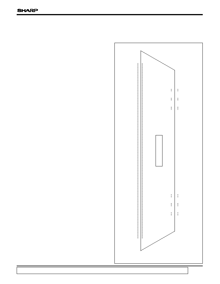
∑ Package : 395-pin TCP (Tape Carrier Package)
PIN CONNECTIONS
LH168K
LH168K
324-output TFT-LCD Source Driver IC
XO
108
YO
108
ZO
108
322
323
324
XO
1
YO
1
ZO
1
1
2
3
CHIP SURFACE
GND
V
LS
GND
MODE
PBS
XB
5
XB
0
XA
5
XA
0
YA
5
YA
0
SPOI
VH
0
VH
8
VH
16
VH
24
VH
32
VH
40
VH
48
VH
56
VH
63
VL
63
VL
56
VL
48
VL
40
VL
32
VL
24
VL
16
VL
8
VL
0
POLB
POLA
CK
SPIO
LS
REV
2
REV
YB
5
YB
0
ZB
5
ZB
0
ZA
5
ZA
0
LBR
V
CC
V
LS
GND
395
394
393
392
391
390
385
384
379
378
373
372
371
370
369
368
367
366
365
364
363
362
361
360
359
358
357
356
355
354
353
352
351
350
349
348
347
346
341
340
335
334
329
328
327
326
325
395-PIN TCP
TOP VIEW
NOTE :
Doesn't prescribe TCP outline.
LH168K
2
PIN DESCRIPTION
PIN NO.
SYMBOL
I/O
DESCRIPTION
1 to 324
XO
1
-ZO
108
O
LCD drive output pins
325, 393, 395
GND
≠
Ground pins
326, 394
V
LS
≠
Power supply pins for analog circuit
327
V
CC
≠
Power supply pin for digital circuit
328
LBR
I
Shift direction selection input pin
329 to 334
ZA
0
-ZA
5
I
Data input pins
335 to 340
ZB
0
-ZB
5
I
Data input pins
341 to 346
YB
0
-YB
5
I
Data input pins
347, 348
REV, REV
2
I
LCD drive output polarity exchange input pins
349
LS
I
Latch input pin
350
SPIO
I/O
Start pulse input/cascade output pin
351
CK
I
Shift clock input pin
352, 353
POLA, POLB
I
Input data polarity exchange input pins
354 to 362
VL
0
-VL
63
I
Reference voltage input pins
363 to 371
VH
63
-VH
0
I
Reference voltage input pins
Data input pins
I
XB
0
-XB
5
385 to 390
Data input pins
I
XA
0
-XA
5
379 to 384
Data input pins
I
YA
0
-YA
5
373 to 378
Start pulse input/cascade output pin
I/O
SPOI
372
392
MODE
I
Input pin for selecting the number of LCD drive outputs
391
PBS
I
2-port/1-port selection input pin
LH168K
4
FUNCTIONAL OPERATIONS OF EACH BLOCK
BLOCK
FUNCTION
Shift Register
Used as a bi-directional shift register which performs the shifting operation by CK and
selects bits for data sampling.
Data Latch
Used to temporary latch the input data which is sent to the sampling memory.
Sampling Memory
Used to sample the data to be entered by time sharing.
Hold memory
Used for latch processing of data in the sampling memory by LS input.
Level Shifter
Used to shift the data in the hold memory to the power supply level of the analog circuit
unit and sends the shifted data to DA converter.
Reference Voltage
Generation Circuit
Used to generate a gamma-corrected 64 x 2-level voltage by the resistor dividing circuit.
DA Converter
Used to generate an analog signal according to the display data and sends the signal to
the output circuit.
Output Circuit
Used as a voltage follower, configured with an operational amplifier and an output buffer,
which outputs analog signals of 64 x 2 gray scales to LCD drive output pin.
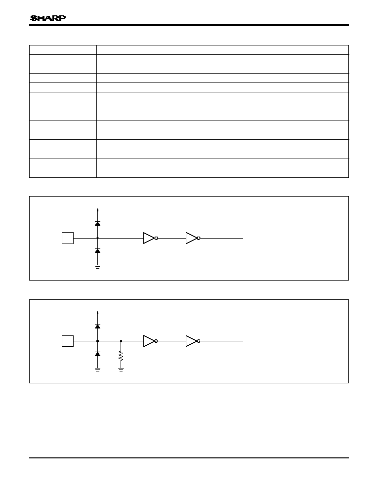
INPUT/OUTPUT CIRCUITS
I
V
CC
GND
To Internal Circuit
Fig. 1 Input Circuit (1)
øApplicable pins°
CK, LS, REV, LBR,
MODE, PBS,
XA
0
-XA
5
, XB
0
-XB
5
,
YA
0
-YA
5
, YB
0
-YB
5
,
ZA
0
-ZA
5
, ZB
0
-ZB
5
I
V
CC
GND
To Internal Circuit
GND
Fig. 2 Input Circuit (2)
øApplicable pins°
POLA, POLB, REV
2

