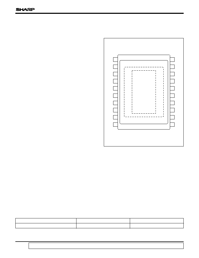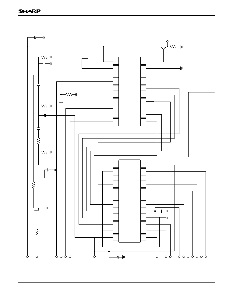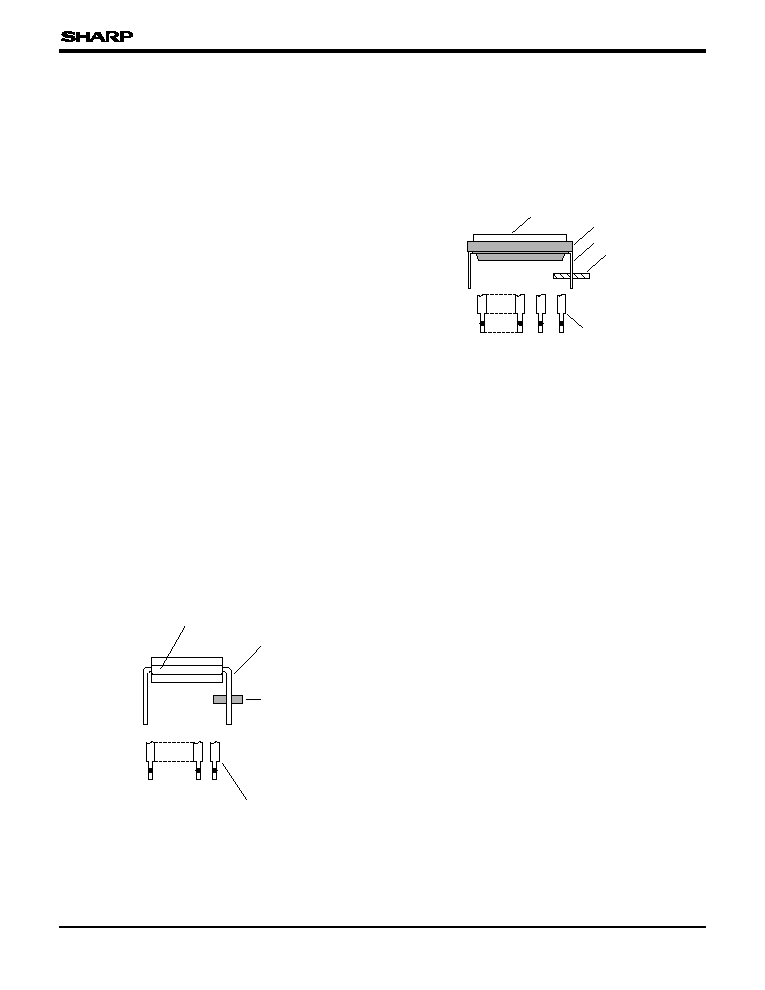
PACKAGES FOR CCD AND CMOS DEVICES
16
,,,,,,,,,,,,,,,,,,,,,,,,,,,,,,,,,,,,,,,,,,,,,,,,,,,,,,,,,,,,,,,,,,,,,,
,,,,,,,,,,,,,,,,,,,,,,,,,,,,,,,,,,,,,,,,,,,,,,,,,,,,,,,,,,,,,,,,,,,,,,
,,,,,,,,,,,,,,,,,,,,,,,,,,,,,,,,,,,,,,,,,,,,,,,,,,,,,,,,,,,,,,,,,,,,,,
,,,,,,,,,,,,,,,,,,,,,,,,,,,,,,,,,,,,,,,,,,,,,,,,,,,,,,,,,,,,,,,,,,,,,,
,,,,,,,,,,,,,,,,,,,,,,,,,,,,,,,,,,,,,,,,,,,,,,,,,,,,,,,,,,,,,,,,,,,,,,
,,,,,,,,,,,,,,,,,,,,,,,,,,,,,,,,,,,,,,,,,,,,,,,,,,,,,,,,,,,,,,,,,,,,,,
,,,,,,,,,,,,,,,,,,,,,,
,,,,,,,,,,,,,,,,,,,,,,
,,,,,,,,,,,,,,,,,,,,,,
,,,,,,,,,,,,,,,,,,,,,,
,,,,,,,,,,,,,,,,,,,,,,
,,,,,,,,,,,,,,,,,,,,,,
,,,,,,,,,,,,,,,,,,,,,,
,,,,,,,,,,,,,,,,,,,,,,
,,,,,,,,,,,,,,,,,,,,,,
,,,,,,,,,,,,,,,,,,,,,,
,,,,,,,,,,,,,,,,,,,,,,
,,,,,,,,,,,,,,,,,,,,,,
,,,,,,,,,,,,,,,,,,,,,,
,,,,,,,,,,,,,,,,,,,,,,
,,,,,,,,,,,,,,,,,,,,,,
,,,,,,,,,,,,,,,,,,,,,,
,,,,,,,,,,,,,,,,,,,,,,
,,,,,,,,,,,,,,,,,,,,,,
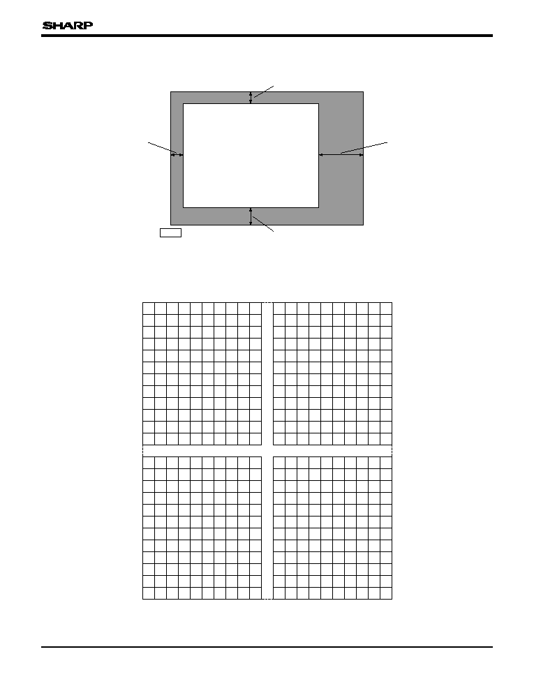
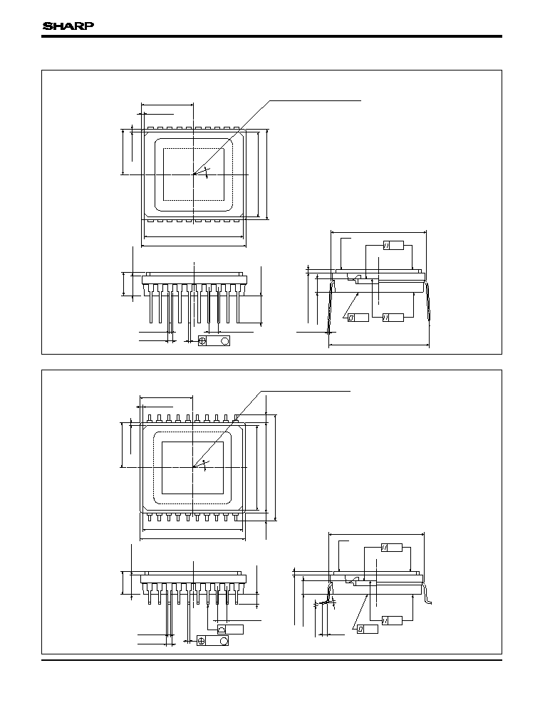
Glass Lid
Package
6.90
Ī0.075
0.40
Ī0.40
6.00
Ī0.075
0.40
Ī0.40
11.20
Ī0.10
(2)
12.00
Ī0.10
13.80
Ī0.10
13.00
Ī0.10
(2)
1
10
CCD
20
11
¨
Center of effective imaging area
and center of package
Rotation error of die : ¨ = 1.0į
MAX.
( 1 : Effective imaging area)
( 2 : Lid's size)
12.20
Ī0.10
Refractive index : nd = 1.5
0.50
Ī0.05
(2)
1.41
Ī0.05
0.25
Ī0.10
12.20
0.04
0.02
0.02
(1)
(1)
A'
A
A
A'
0.64
TYP.
0.30
TYP.
P-1.27
TYP.
0.20 M
3.50
Ī0.10
2.40
Ī0.10
2.90
Ī0.10
CCD
+0.30
≠0
20 WDIP (WDIP020-P-0500)
PACKAGES
(Unit : mm)
,,,,,,,,,,,,,,,,,,,,,,,,,,,,,,,,,,,,,,,,,,,,,,,,,,,,,,,,,,,,,,,,,,,,,,
,,,,,,,,,,,,,,,,,,,,,,,,,,,,,,,,,,,,,,,,,,,,,,,,,,,,,,,,,,,,,,,,,,,,,,
,,,,,,,,,,,,,,,,,,,,,,,,,,,,,,,,,,,,,,,,,,,,,,,,,,,,,,,,,,,,,,,,,,,,,,
,,,,,,,,,,,,,,,,,,,,,,,,,,,,,,,,,,,,,,,,,,,,,,,,,,,,,,,,,,,,,,,,,,,,,,
,,,,,,,,,,,,,,,,,,,,,,,,,,,,,,,,,,,,,,,,,,,,,,,,,,,,,,,,,,,,,,,,,,,,,,
,,,,,,,,,,,,,,,,,,,,,,,,,,,,,,,,,,,,,,,,,,,,,,,,,,,,,,,,,,,,,,,,,,,,,,
,,,,,,,,,,,,,,,,,,,,,,,,,,,,,,,,,,,,,,,,,,,,,,,,,,,,,,,,,,,,,,,,,,,,,,
,,,,,,,,,,,,,,,,,,,,,,
,,,,,,,,,,,,,,,,,,,,,,
,,,,,,,,,,,,,,,,,,,,,,
,,,,,,,,,,,,,,,,,,,,,,
,,,,,,,,,,,,,,,,,,,,,,
,,,,,,,,,,,,,,,,,,,,,,
,,,,,,,,,,,,,,,,,,,,,,
,,,,,,,,,,,,,,,,,,,,,,
,,,,,,,,,,,,,,,,,,,,,,
,,,,,,,,,,,,,,,,,,,,,,
,,,,,,,,,,,,,,,,,,,,,,,
,,,,,,,,,,,,,,,,,,,,,,,
,,,,,,,,,,,,,,,,,,,,,,,
,,,,,,,,,,,,,,,,,,,,,,,
,,,,,,,,,,,,,,,,,,,,,,,
,,,,,,,,,,,,,,,,,,,,,,,
,,,,,,,,,,,,,,,,,,,,,,,
Glass Lid
Package
6.90
Ī0.075
0.40
Ī0.40
6.00
Ī0.075
0.40
Ī0.40
11.20
Ī0.10
(2)
12.00
Ī0.10
(1.00)
(1.00)
14.00
Ī0.10
13.80
Ī0.10
13.00
Ī0.10
(2)
1
10
CCD
20
11
¨
Center of effective imaging area
and center of package
Rotation error of die : ¨ = 1.0į
MAX.
( 1 : Effective imaging area)
( 2 : Lid's size)
12.20
Ī0.10
Refractive index : nd = 1.5
0.50
Ī0.05
(2)
1.41
Ī0.05
0.25
Ī0.10
0.83
CCD
0.04
0.02
0.02
(1)
(1)
A'
A
1-5į
A
A'
P-1.27
TYP.
0.64
TYP.
0.30
TYP.
0.10
0.20 M
1.00
Ī0.10
2.40
Ī0.10
2.90
Ī0.10
20 WSOP (WSOP020-P-0525)