 | ÐлекÑÑоннÑй компоненÑ: PC352 | СкаÑаÑÑ:  PDF PDF  ZIP ZIP |
/home/web/doc/html/sharp/184511
PC352
PC352
s
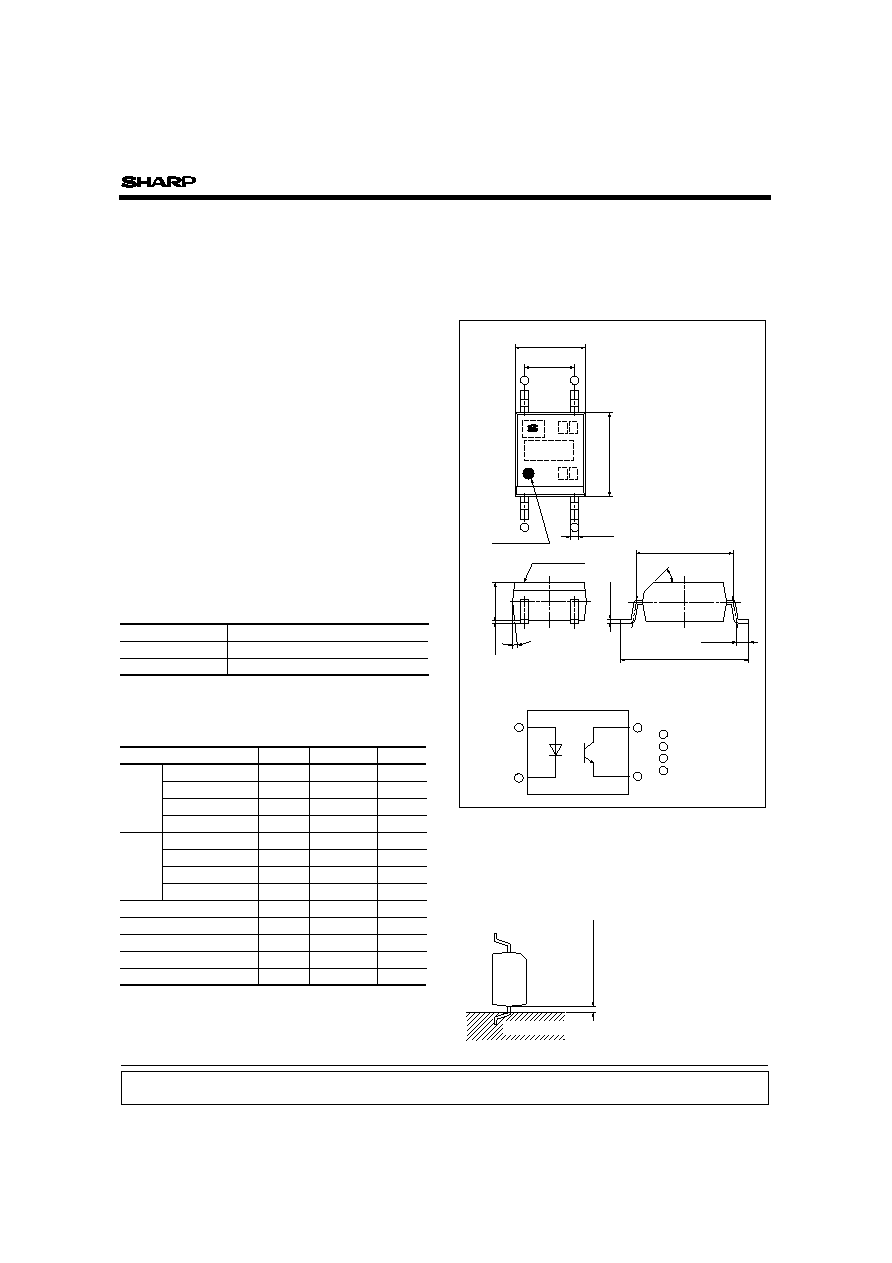
Package Specifications
s
Outline Dimensions
(Unit : mm)
Opaque
*
, Mini-flat Package,
High Resistance to Noise Type
Photocoupler
1. Programmable controllers
s
Features
s
Applications
1. Opaque type, mini-flat package
PC352
(1-channel)
2. High resistance to noise due to high common mode
rejection voltage (V
CM
: TYP. 1.5kV)
3. Subminiature type
(The volume is smaller than that of our
conventional DIP type by as far as 30%.)
4. Isolatin voltage between input and output
PC352
···Viso(rms) : 3.75kV
5. Recognized by UL, file No. E64380
* Employs double transfer mold technology
Model No.
Package specification
PC352N
PC352NT
Taping reel diameter 178mm (750 pcs)
Taping reel diameter 370mm (3 000 pcs)
s
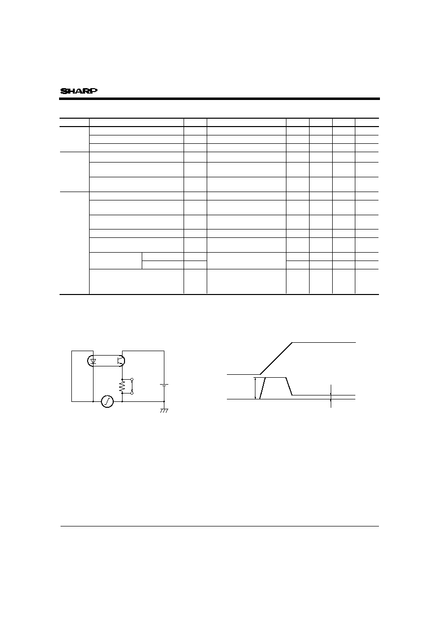
Absolute Maximum Ratings
0.2mm or more
Soldering area
Notice
In the absence of confirmation by device specification sheets, SHARP takes no responsibility for any defects that may occur in equipment using any SHARP
devices shown in catalogs, data books, etc. Contact SHARP in order to obtain the latest device specification sheets before using any SHARP device.
Internet
Internet address for Electronic Components Group http://www.sharp.co.jp/ecg/
Parameter
Symbol
Rating
Unit
Input
Forward current
50
1
mA
A
6
V
Output
70
150
mW
mW
170
mW
35
6
V
V
50
mA
-
30 to
+
100
°C
Storage temperature
-
40 to
+
125
°C
260
°C
Operating temperature
Reverse voltage
Peak forward current
Power dissipation
Collector-emitter voltage
Emitter-collector voltage
Collector current
Collector dissipation
I
F
V
R
I
FM
P
V
CEO
V
ECO
I
C
P
C
T
stg
T
opr
P
tot
(Ta=25°C)
Soldering temperature
T
SOL
3.75
kV
Isolation voltage
V
iso
(rms)
*1
*1
*1
*1
*1
*3
*4
*2
*1 The derating factors of absolute maximum ratings due to ambient temperature
are shown in Fig.2 to 5
*2 Pulse width
100
µ
s, Duty ratio:0.01, Refer to Fig.6
*3 AC for 1min., 40 to 60% RH, f=60Hz
*4 For 10s
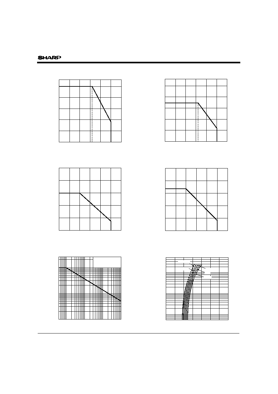
Total power dissipation
3 5 2
4
3
1
2
1
2
4
3
4.4
±
0.2
5.3
±
0.3
2.6
±
0.2
0.1
±
0.1
3.6
±
0.3
2.54
±
0.25
0.4
±
0.1
0.5
+
0.4
-
0.2
7.0
+
0.2
-
0.7
Anode mark
Epoxy resin
45
°
6
°
Internal connection diagram
0.2
±
0.05
1
2
3
4
Anode
Anode
Cathode
Emitter
Collector
PC352
s
Electro-optical Characteristics
Parameter
Conditions
Input
Forward voltage
I
F
=
20mA
V
R
=
4V
Terminal capacitance
Output
Collector-emitter
I
C
=
0.1mA, I
F
=
0
Emitter-collector
I
E
=
10
µ
A, I
F
=
0
I
F
=
0, R
L
=
470
Vnp
=
100mV
V
CM
=1.5kV(peak)
Transfer
charac-
teristics
Collector current
I
F
=
5mA, V
CE
=
5V
Collector-emitter
saturation voltage
I
F
=
20mA, I
C
=
1mA
Isolation resistance
DC500V
40 to 60%RH
Floating capacitance
Cut-off frequency
Common mode rejection voltage
V
=
0, f
=
1MHz
Response time
Rise time
Fall time
MIN.
-
-
-
-
-
35
6
4.5
-
5
×
10
10
-
-
-
TYP.
1.2
30
-
-
-
-
0.1
1
×
10
11
0.6
4
5
MAX.
1.4
10
200
100
-
-
24
0.2
-
1.0
15
80
-
18
20
Collector dark current
breakdown voltage
breakdown voltage
Symbol
V
F
I
R
C
t
I
CEO
BV
CEO
BV
ECO
I
C
V
CE(sat)
C
f
f
c
t
r
t
f
R
ISO
CMR
V
=
0, f
=
1kHz
Unit
V
nA
µ
A
V
V
mA
10
-
-
kV/
µ
s
V
pF
pF
µ
s
µ
s
V
CE
=
2V, I
C
=
2mA
R
L
=
100
V
CE
=
5V, I
C
=
2mA
R
L
=
100
,
-
3dB
(Ta
=
25°C)
V
CE
=
20V, I
F
=
0
Reverse current
*5 Refer to Fig.1
*5
Fig.1 Test Circuit for Common Mode Rejection Voltage
V
CM
V
cp
V
np
V
O
(dV/d
t
)
1)
R
L
V
np
V
CC
V
CM
1) V
cp
: Voltage which is generated by displacement current in floating
capacitance between primary and secondary side.
(V
cp
Nearly
=
dV/d
t
×
C
f
×
R
L
)
V
CM :
High wave
pulse
R
L
=
470
V
CC
=
9V
PC352
Forward voltage V
F
(V)
50
°C
25
°C
0
°C
0
2
0.5
1.0
1.5
2.0
2.5
3.0
3.5
5
10
20
50
100
200
500
1
-
25
°C
Ta
=
75°C
Forward current I
F
(mA)
Peak forward current I
FM
(mA)
10
20
50
100
200
2000
500
1000
5
2
10
-
3
5
2
10
-
2
5
2
10
-
2
5
1
Duty ratio
Pulse width
100
µ
s
T
a
=
25
°
C
Total power dissipation P
tot
(mW)
0
50
100
150
200
250
170
-
30
0
25
50
75
100
125
Ambient temperature T
a
(
°
C)
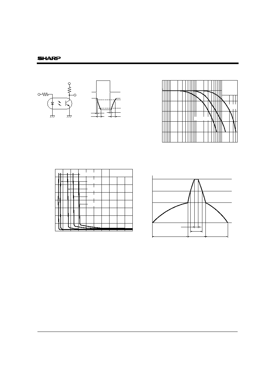
Fig.5 Total Power Dissipation vs. Ambient
Temperature
Collector power dissipation P
C
(mW)
0
50
100
150
200
250
-
30
0
25
50
75
100
125
Ambient temperature T
a
(
°
C)
Fig.4 Collector Power Dissipation vs.
Ambient Temperature
Fig.7 Forward Current vs. Forward Voltage
Fig.6 Peak Forward Current vs. Duty Ratio
Forward current I
F
(mA)
0
10
20
30
40
50
-
30
0
25
75
100
125
55
50
Ambient temperature T
a
(
°
C)
0
20
40
60
70
80
100
-
30
0
25
75
100
125
55
50
Ambient temperature T
a
(
°
C)
Diode power dissipation P (mW)
Fig.2 Forward Current vs. Ambient
Temperature
Fig.3 Diode Power Dissipation vs. Ambient
Temperature
PC352
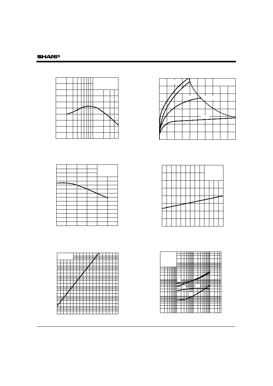
Relative current transfer ratio (%)
Ambient temperature T
a
(
°
C)
100
0
50
150
0
25
50
75
-
30
100
125
I
F
=5mA
V
CE
=5V
Response time (
µ
s)
Load resistance R
L
(k
)
0.2
0.1
0.5
1
2
5
10
20
0.01
0.1
1
10
50
50
100
200
500
V
CE
=2V
I
C
=2mA
T
a
=25°C
t
f
t
r
t
d
t
s
Collector-emitter saturation
voltage V
CE
(sat) (V)
Ambient temperaturet T
a
(
°
C)
0
-
30
0.02
0
20
40
60
80
100
0.04
0.06
0.08
0.10
0.12
0.14
0.16
I
F
=20mA
I
C
=1mA
Collector dark current I
CEO
(A)
Ambient temperature T
a
(
°
C)
20
0
40
60
80
100
-
30
V
CE
=20V
120 140
10
-
7
10
-
6
10
-
8
10
10
10
10
-
9
-
10
-
11
-
12
Fig.10 Relative Current Transfer Ratio vs.
Ambient Temperature
Fig.11 Collector-emitter Saturation
Voltage vs. Ambient Temperature
Fig.13 Response Time vs. Load Resistance
Fig.12 Collector Dark Current vs. Ambient
Temperature
Current transfer ratio CTR (%)
Forward current I
F
(mA)
0
1
500
2
5
10
20
50
400
300
200
100
V
CE
=5V
T
a
=25°C
Collector current I
C
(mA)
Collector-emitter voltage V
CE
(V)
0
0
5
1
10
15
20
25
30
35
40
2
3
4
5
6
7
8
9
10
20mA
10mA
5mA
I
F
=30mA
T
a
=25°C
P
C
(MAX.)
Fig.8 Current Transfer Ratio vs. Forward
Current
Fig.9 Collector Current vs. Collector-emitter
Voltage
PC352
Fig.14 Test Circuit for Response Time
Forward current I
F
(mA)
Collector-emitter saturation voltage
V
CE
(sat) (V)
0
0
2
4
6
8
2
4
6
8
10
1mA
3mA
7
5
3
1
9
7
5
3
1
5mA
7mA
T
a
=25°C
I
C
=0.5mA
Fig.16 Collector-emitter Saturation Voltage
vs. Forward Current
Fig.17 Reflow Soldering
Voltage gain A
V
(dB)
Frequency Response f (kHz)
0
0.5
1
2
5
200
100
50
20
10
500
100
1k
-
5
-
10
-
15
-
20
R
L
=10k
V
CE
=5V
I
C
=2mA
T
a
=25°C
Fig.15 Voltage Gain vs Frequency
10%
Input
Output
Input
Output
90%
t
s
t
d
V
CC
R
D
R
L
t
f
t
r
25
°
C
2min
230
°
C
200
°
C
180
°
C
1min
1min
1.5min
30s
Only one time soldering is recommended within the temperature
profile shown below.