 | –≠–ª–µ–∫—Ç—Ä–æ–Ω–Ω—ã–π –∫–æ–º–ø–æ–Ω–µ–Ω—Ç: PC852 | –°–∫–∞—á–∞—Ç—å:  PDF PDF  ZIP ZIP |
PC853/PC853H
PC852 Series
PC852 Series/PC853/PC853H
s
Applications
s
Features
1. High collector-emitter voltage
2. High current transfer ratio
3. High isolation voltage between input and
output ( V
iso
4. Compact dual-in-line package
5. Large collector power dissipation.
6. Recognized by UL
1. Telephone sets
2. Copiers, facsimiles
3. Interface with various power supply cir-
cuits, power distribution boards
4. Numerical control machines
F
= 1mA, V
CE
= 2V)
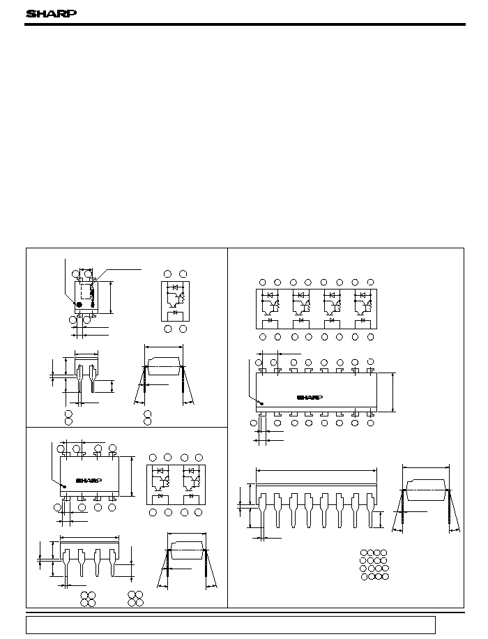
( Unit : mm)
s
Outline Dimensions
PC852
,
PC853
,
PC853H
( 1-channel type )
data books, etc. Contact SHARP in order to obtain the latest version of the device specification sheets before using any SHARP's device.
"
"
In the absence of confirmation by device specification sheets, SHARP takes no responsibility for any defects that occur in equipment using any of SHARP's devices, shown in catalogs,
PC8Q52
PC8D52
Internal connection
diagram
diagram
Internal connection
PC8D52
Internal connection
diagram
2
1
4
3
Anode mark
PC
Model No
PC852/PC853/PC853H
1
2
3
4
3 Emitter
4 Collector
1
2
3
4
5
6
7
8
1
2
3
4
5
6
7
8
1 3 Anode
2 4 Cathode
5 7 Emitter
6 8 Collector
Anode mark
1
2
3
4
5
6
7
8
9
PC8Q52
1
2
3
4
5
6
7
8
9
Anode mark
1 3 5 7 Anode
2 4 6 8 Cathode
9
Emitter
Collector
(Note)
1 Anode
2 Cathode
PC852 Series
,
PC853
( V
CEO
: 300V)
PC853H
( V
CEO
: 350V)
PC8D52
( 2-channel type )
PC8Q52
( 4-channel type )
PC853
,
PC853H
(P
C
: 300mW )
High Collector-emitter Voltage
Type Photocouplers
The diode of output side is not a protection diode
( CTR: MIN. 1 000% at I
of reverse voltage.
g Lead forming type ( I type ) and taping reel type ( P type ) are also available. (
PC852I/PC852P/PC853I/PC853P
)
: 5 000V
rms
)
=
0 to 13
∞
6.5
±
0.5
2.54
±
0.25
0.9
±
0.2
1.2
±
0.3
4.58
±
0.5
3.0
±
0.5
0.5
±
0.1
3.3
±
0.5
3.5
±
0.5
0.5
TYP.
7.62
±
0.3
0.26
±
0.1
6.5
±
0.5
2.54
±
0.25
0.9
±
0.2
1.2
±
0.3
9.66
±
0.5
3.5
±
0.5
3.3
±
0.5
0.5
TYP.
0.5
±
0.1
3.0
±
0.5
=
0 to 13
∞
6.5
±
0.5
0.9
±
0.2
1.2
±
0.3
19.82
±
0.5
7.62
±
0.3
0.26
±
0.1
3.0
±
0.5
0.5
±
0.1
3.5
±
0.5
3.3
±
0.5
0.5
TYP.
2.54
±
0.25
=
0 to 13
∞
7.62
±
0.3
0.26
±
0.1
11
12
13
14
15
16
11
12
13
14
15
16
11
12
13
14
15
16
10
10
10
( NO. E64380 )
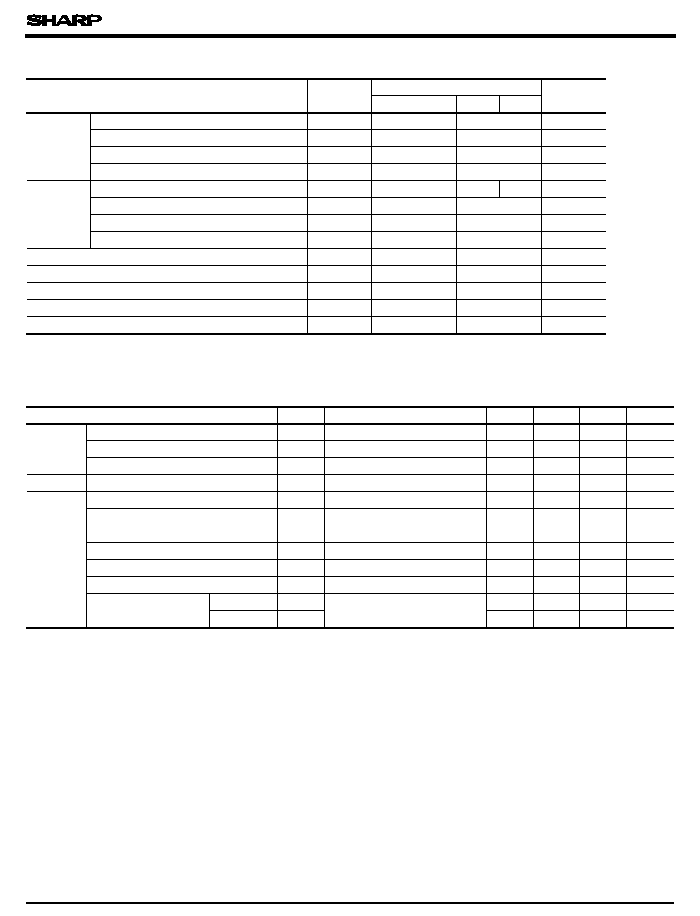
PC852 Series /PC853/PC853H
Parameter
Symbol
Rating
Unit
PC853
Input
Forward current
I
F
50
50
mA
I
FM
1
1
A
Reverse voltage
V
R
6
6
V
Power dissipation
P
70
70
mW
Output
Collector-emitter voltage
V
CEO
300
300
350
V
Emitter-collector voltage
V
ECO
0.1
0.1
V
Collector current
I
C
150
150
mA
Collector power dissipation
P
C
150
300
mW
Total power dissipation
P
tot
200
320
mW
V
iso
V
rms
Operating temperature
T
opr
- 30 to + 100
- 30 to + 100
∞C
Storage temperature
T
stg
- 55 to + 125
- 55 to + 125
∞C
T
sol
260
260
∞C
*3 For 10 seconds
*1
Peak forward current
*2
Isolation voltage
*3
Soldering temperature
s
Electro-optical Characteristics
*1 Pulse width<=100
µ
s, Duty ratio : 0.001
Parameter
Symbol
Conditions
MIN.
TYP.
MAX.
Unit
Input
Forward voltage
V
F
I
F
= 10mA
-
1.2
1.4
V
Reverse current
I
R
V
R
= 4V
-
-
10
µ
A
Terminal capacitance
C
t
V = 0, f = 1kHz
-
30
250
pF
Output
Collector dark current
I
CEO
V
CE
= 200V, I
F
= 0
-
-
2 x 10
- 7
A
Transfer
charac-
teristics
Current transfer ratio
CTR
I
F
= 1mA, V
CE
= 2V
%
Collector-emitter
saturation voltage
V
CE( sat )
I
F
= 20mA, I
C
= 100mA
-
-
1.2
V
Isolation resistance
R
ISO
5 x 10
10
10
11
-
Floating capacitance
-
0.6
1.0
pF
Cut-off frequency
f
c
V
CE
= 2V, I
C
= 20mA, R
L
= 100
, - 3dB
1
7
-
kHz
Response time
Rise time
t
r
V
CE
= 2V, I
C
= 20mA
-
100
300
µ
s
Fall time
-
20
100
µ
s
( Ta = 25∞C)
( Ta = 25∞C)
PC853H
PC852
Series
C
f
t
f
s
Absolute Maximum Ratings
5 000
5 000
*2 40 to 60% RH, AC for 1 minute
1 000
4 000
15 000
DC500V, 40 to 60% RH
V = 0, f = 1MHz
R
L
= 100
0
- 30
10
0
25
50
75
100
125
20
30
40
50
60
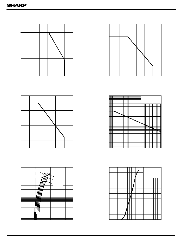
Fig. 1 Forward Current vs.
Ambient Temperature
Ambient temperature T
a
(∞C)
0
0
125
100
200
50
150
25
50
75
100
- 30
- 25
0
25
50
75
100
125
0
50
100
150
200
250
300
350
Collector power dissipation P
C
(
mW
)
Ambient temperature T
a
(∞C)
Duty ratio
5
5
Pulse width <=100
µ
s
10
20
100
50
200
500
2
10
- 3
10
- 2
5
2
10
- 1
5
2
5
Fig. 3 Peak Forward Current vs. Duty Ratio
Peak forward current I
FM
(
mA
)
0
2
0.5
1.0
1.5
2.0
2.5
3.0
3.5
5
10
20
50
100
200
500
1
Forward voltage V
F
(V)
Fig. 4 Forward Current vs. Forward Voltage
0
0.1
Current transfer ratio CTR
(
%
)
0.2
0.5
10
1
2
5
Forward current I
F
( mA )
Ambient Temperature
Ambient Temperature
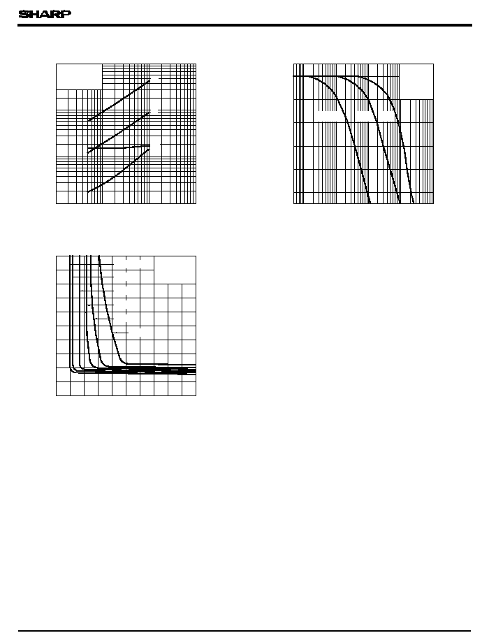
PC852 Series/PC853/PC853H
Forward current I
F
(
mA
)
(
PC852 Series
)
Collector power dissipation P
C
(
mW
)
(
PC853/PC853H
)
Forward current I
F
(
mA
)
(
PC852 Series
)
Forward Current
Fig. 2-a Collector Power Dissipation vs.
Fig. 2-b Collector Power Dissipation vs.
Fig. 5-a Current Transfer Ratio vs.
1
50∞C
25∞C
0∞C
- 25∞C
T
a
= 75∞C
V
CE
= 2V
T
a
= 25∞C
Ambient temperature T
a
( ∞C )
10 000
5 000
2 000
1 000
T
a
= 25∞C
5 000
4 000
3 000
2 000
1 000

Forward current I
F
( mA )
0
0.1
Current transfer ratio CTR
(
%
)
0.2
0.5
1
2
5
10
0
0
100
200
1
2
3
4
5
0.5mA
1mA
1.5mA
2mA
2.5mA
3mA
5mA
Collector-emitter Voltage
Collector current I
C
(
mA
)
Collector-emitter voltage V
CE
(V)
0
0
100
200
1
2
3
4
5
Collector current I
C
(
mA
)
Collector-emitter voltage V
CE
(V)
Collector-emitter Voltage
50
0
100
150
0
20
40
60
80
100
50
0
100
150
0
Relative current transfer ratio
(
%
)
0
- 30
0.2
0
20
40
60
80
100
0.4
0.6
0.8
1.0
1.2
Fig. 8 Collector-emitter Saturation
Voltage vs. Ambient Temperature
Ambient temperature T
a
(∞C)
CE
( sat
)
(
V
)
20
0
40
60
-11
80
100
10
-10
10
-9
10
-8
10
-7
10
-6
10
-5
Fig. 9 Collector Dark Current vs.
Ambient Temperature
Collector dark current I
CEO
(
A
)
Ambient temperature T
a
( ∞C)
PC852 Series/PC853/PC853H
Forward Current
(
PC853/PC853H
)
(
PC852 Series
)
(
PC853
/
PC853H
)
P
C
( MAX. )
Fig. 5-b Current Transfer Ratio vs.
Fig. 6-a Collector Current vs.
Fig. 6-b Collector Current vs.
Fig. 7 Relative Current Transfer Ratio vs.
Ambient Temperature
Ambient Temperature T
a
( ∞C )
Collector-emitter saturation voltage V
0.5mA
1mA
1.5mA
2mA
2.5mA
3mA
5mA
V
CE
= 2V
T
a
= 25∞C
T
a
= 25∞C
I
F
= 10mA
T
a
= 25∞C
P
C
( MAX. )
I
F
= 10mA
I
F
= 1mA
V
CE
= 2V
I
F
= 20mA
I
C
= 100mA
V
CE
= 200V
5 000
4 000
3 000
2 000
1 000
- 30
- 30
10
Response time
(
µ
s
)
2
1
5
10
20
50
100
200
500
0.01
0.1
1
10
Fig.11 Frequency Response
Frequency f ( kHz )
0
0.1
1
10
100
100
10
Voltage gain A
v
(
dB
)
Collector-emitter saturation voltage V
CE
( sat
)
(V
)
Forward current I
F
( mA )
0
0
1
2
3
4
5
1
2
3
4
5
10mA
30mA
50mA
70mA
100mA
Fig.12 Collector-emitter Saturation
Voltage vs. Forward Current
PC852 Series/PC853/PC853H
V
CE
= 2V
I
C
= 20mA
T
a
= 25∞C
t
r
t
f
t
d
t
s
V
CE
= 2V
I
C
= 20mA
T
a
= 25∞C
T
a
= 25∞C
R
L
= 1k
I
C
= 5mA
1 000
1 000
- 25
- 20
- 15
- 10
- 5
Please refer to the chapter " Precautions for Use "
Fig.10 Response Time vs. Load Resistance
Load resistance R
L
( k
)
q