PQ1CG3032FZ/
PQ1CG3032RZ
PQ1CG3032FZ/PQ1CG3032RZ
s
Absolute Maximum Ratings
s
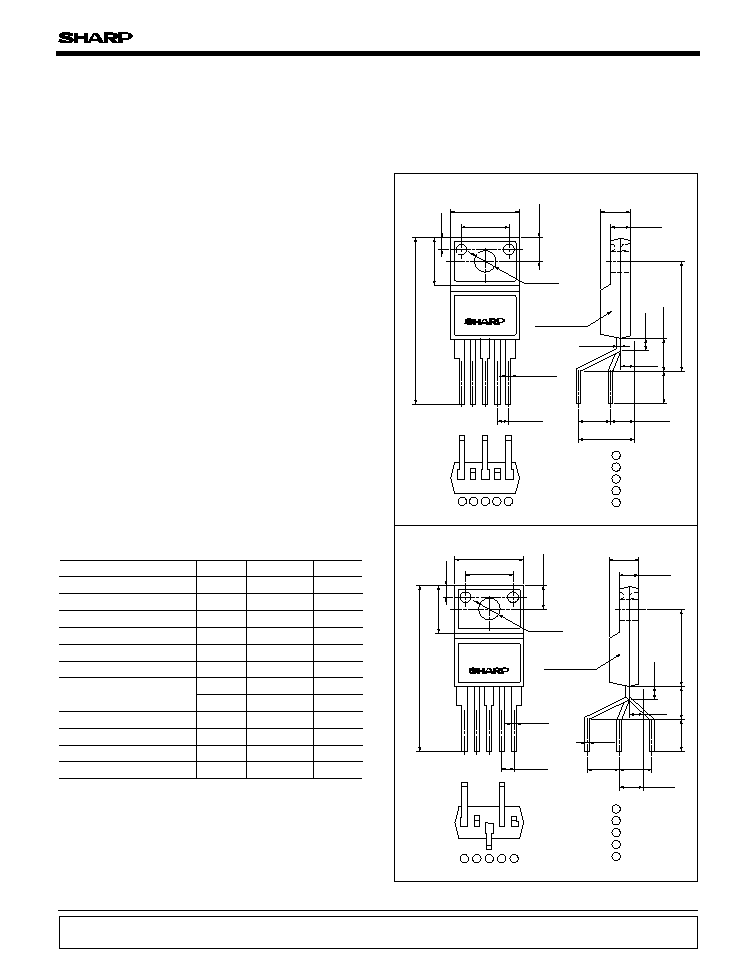
Outline Dimensions
(Unit : mm)
Parameter
Symbol
Rating
Unit
Input voltage
40
V
3.5
A
1.4
7
41
-
1
V
V
V
W
V
-
0.3 to
+
40
Switching current
150
�C
-
20 to
+
80
�C
Junction temperature
Dropout voltage
Output-COM voltage
Output adjustment terminal voltage
V
IN
V
I-O
V
OUT
ON/OFF control voltage
V
C
V
ADJ
I
SW
T
j
(Ta
=
25
�
C)
Operating temperature
Storage temperature
Soldering temperature
T
opr
-
40 to
+
150
�C
T
stg
260
�C
T
sol
*2
*3
*1
*5
*6
Power dissipation
P
D1
14
W
P
D2
*4
*1 Voltage between V
IN
terminal and COM terminal
*2 Voltage between V
OUT
terminal and COM terminal
*3 Voltage between ON/OFF control and COM terminal
*4 P
D
:With infinite heat sink
*5 Over heat protection may operate at the condition T
j
=
125�C to 150�C
*6 For 10s
1. CTV
2. Digital OA equipment
3. Facsimiles, printers and other OA equipment
4. Personal computers and amusement equipment
s
Features
s
Applications
TO-220 Type Chopper Regulator
1. Maximum switching current:3.5A
2. Built-in ON/OFF control function
3. Built-in soft start function to suppress overshoot of output
voltage in power on sequence or ON/OFF control sequence
4. Built-in oscillation circuit
(Oscillation frequency:TYP. 150kHz)
5. Built-in overheat/overcurrent protection function
6. TO-220 package
7. Variable output voltage
(Output variable range:V
ref
to 35V/
-
V
ref
to
-
30V)
[Possible to select step-down output/inversing output
according to external connection circuit]
8.
PQ1CG3032FZ
:Zigzag forming
PQ1CG3032RZ
:Self-stand forming
Notice
In the absence of confirmation by device specification sheets, SHARP takes no responsibility for any defects that may occur in equipment using any SHARP
devices shown in catalogs, data books, etc. Contact SHARP in order to obtain the latest device specification sheets before using any SHARP device.
Internet
Internet address for Electronic Components Group http://www.sharp.co.jp/ecg/
(6.8)
4
-
(1.7)
(5.0)
(1.5)
(0.5)
(2.0)
(24.6)
10.2
MAX.
4.4
MIN.
3.6
�
0.2
3.2
�
0.1
4.5
�
0.2
2.8
�
0.2
5.0
�
0.5
16.4
�
0.7
3.2
�
0.1
7.4
�
0.2
(1.5)
5
-
0.8
�0.
1
3.2
�
0.5
8.2
�
0.7
(6.8)
4
-
(1.7)
(1.7)
(2.2)
(24.6)
10.2
MAX.
(11.4)
(3.6)
3.6
�
0.2
4.5
�
0.2
2.8
�
0.2
6.0
�
0.5
7.4
�
0.2
(1.5)
0.8
�0.
1
4.7
�
0.6
4.7
�
0.6
2.6
�
0.5
1
2
3
V
IN
V
OUT
COM
4
5
O
ADJ
ON/OFF
1
2
3
4
5
1
2
3
4
5
1
2
3
V
IN
V
OUT
COM
4
5
O
ADJ
ON/OFF
Epoxy resin
Epoxy resin
(0.5)
( ) : Typical dimensions
( ) : Typical dimensions
PQ1CG3032
PQ1CG3032
PQ1CG3032RZ
PQ1CG3032FZ
PQ1CG3032FZ/PQ1CG3032RZ
Parameter
Symbol
Conditions
V
SAT
V
ref
V
ref
|R
eg
L|
|R
eg
I|
f
O
I
L
Unit
MAX.
TYP.
MIN.
-
-
-
-
-
-
-
-
-
1.235
135
0.7
0.8
0.9
3.6
I
SW
=
3A
-
T
j
=
0 to 125�C
I
O
=
0.5 to 3A
V
IN
=
8 to 35V
I
O
=
3A
-
1.4
1.26
�
0.5
0.2
1
80
150
�
2
4.7
1.8
1.285
1.5
2.5
165
5.8
(Unless otherwise specified, condition shall be V
IN
=
12V, I
O
=
0.5A, V
O
=
5V, ON-OFF terminals is open,
Ta=25�C)
V
V
%
%
%
%
kHz
%
V
-
140
400
�
A
-
8
16
mA
A
Output saturation voltage
Reference voltage
Reference voltage temperature fluctuation
Load regulation
Line regulation
Efficiency
Oscillation frequency
Oscillation frequency temperature fluctuation
Overcurrent detecting level
ON threshold voltage
Stand-by current
Output OFF-state consumption current
f
O
T
j
=
0 to 125�C
-
V
TH(ON)
-
2.3
-
V
Threshold input voltage
V
THH
-
1.3
-
V
V
THL
-
-
10
-
�
A
Charge current
I
CHG
I
SD
I
QS
V
IN
=
40V, terminal
=
0.9V
Duty ratio
=
100%, terminals is open, terminal
terminal
=
0V, terminal
V
IN
=
40V, terminal
=
0V
Duty ratio
=
0%, terminal
=
0V, terminal
, terminals is open, terminal
4
2
5
5
4
5
4
4
5
5
5
s
Electrical Characteristics
1
2
L
D
5
3
4
R
1
R
2
I
O
I
SD
I
QS
I
CHG
V
O
C
O
+
C
IN
V
IN
+
90
�
H
1 000
�
F
220
�
F
1k
A
V
IN
A
A
L : HK-12S120-9000R (made by Toho Co.)
D : ERC80-004 (made by Fuji electronics Co.)
Load
PQ1CG3032FZ
Fig.1
Standard Test Circuit
Power dissipation P
D
(W)
0
5
10
15
20
-
20
0
25
50
75 80
P
D1
: No heat sink
P
D2
: With infinite heat sink
Ambient temperature T
a
(
�
C)
Note) Oblique line prtion:Overheat protection may operate in this area
Output voltage V
O
(V)
Load current I
O
(A)
0
1
2
3
4
5
6
0
1
2
3
4
5
T
a
=
25
�
C
V
IN
=
12V
V
O
=
5V
Fig.2 Power Dissipation vs. Ambient
Temperature
Fig.3 Overcurrent Protection Characteristics
(Typical Value)
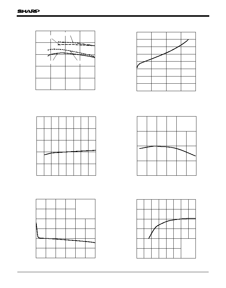
PQ1CG3032FZ/PQ1CG3032RZ
Fig.5 Output Saturation Voltage vs.
Switching Current
Fig.4 Efficiency vs. Input Voltage
Fig.7 Reference Voltage Fluctuation vs.
Junction Temperature
Efficiency (%)
Input voltage V
IN
(V)
50
60
70
80
90
100
0
10
20
30
40
V
O
=
12V, I
O
=
3A
V
O
=
5V, I
O
=
3A
V
O
=
12V, I
O
=
1A
T
j
=
25
�
C
V
O
=
5V, I
O
=
1A
Output saturation voltage V
SAT
(V)
0
1.6
1.4
1.2
1
0.8
0.6
0.4
0.2
0
1
2
3
4
Switching current I
SW
(A)
T
j
=
25
�
C
Fig.9 Line Regulation vs. Input Voltage
Fig.8 Load Regulation vs. Output Current
Load regulation R
eg
L (%)
Output current I
O
(A)
0
0.5
1
1.5
2
2.5
3
-
1
-
0.5
0
0.5
1
1.5
2
T
j
=
25
�
C
V
IN
=
12V
V
O
=
5V
Line regulation R
eg
I
(%)
Input voltage V
IN
(V)
-
1
-
0.5
0
0.5
1
1.5
2
0
10
20
30
40
5
15
25
35
T
j
=
25
�
C
V
O
=
5V
I
O
=
0.5A
Reference voltage fluctuation
V
ref
(%)
-
2
-
1
0
1
2
-
25
0
25
50
75
100
125
Junction temperature T
j
(
�
C)
V
IN
=
12V
V
O
=
5V
Fig.6 Stand by Current vs. Intput Voltage
Stand by current I
SD
(
�
A)
0
50
100
150
200
250
0
5
10
15
20
25
30
40
35
Intput voltage V
IN
(V)
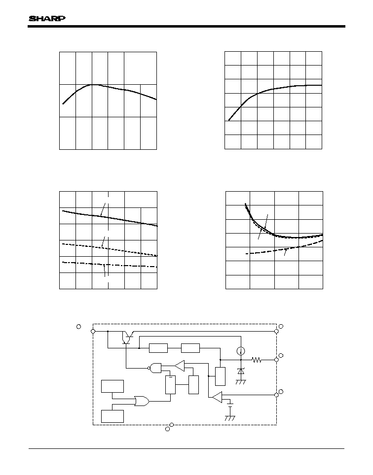
PQ1CG3032FZ/PQ1CG3032RZ
Fig.13 Operating Consumption Current vs.
Input Voltage
Fig.12 Threshold Voltage vs. Junction
Temperature
Fig.14 Block Diagram
Threshold voltage V
TH(ON),
V
TH(L),
V
TH(H)
(V)
0
0.5
1
1.5
2
2.5
3
0
50
100
-
25
25
75
125
Junction temperature T
j
(
�
C)
V
TH(L)
V
TH(H)
V
TH(ON)
V
IN
=
12V
Voltage
regulator
Overcurrent
detection
circuit
Overheat
detection
circuit
ON/OFF
circuit
Q
R
S
F/F
Oscillator
Soft start
2
5
4
1
3
COM
PWM COMP.
ERROR AMP.
V
IN
V
OUT
ON/OFF
O
ADJ
V
ref
-
-
+
+
Operating consumptioon current I
Q'
(mA)
Input voltage V
IN
(V)
5
6
7
8
9
10
11
12
0
10
20
30
40
Tj
=
25
�
C
V
O
=
5V
No load
I
O
=
1A
I
O
=
3A
Oscillation frequency fluctuation
f
O
(%)
-
10
-
5
0
5
-
25
0
25
50
75
100
125
Junction temperature T
j
(
�
C)
V
IN
=
12V
V
O
=
5V
Overcurrent detecting level Fluctuation
I
L
(%)
-
8
-
6
-
4
-
2
0
2
4
6
-
25
0
25
50
75
100
125
Junction temperature T
j
(
�
C)
Fig.10 Oscillation Frequency Fluctuation vs.
Junction Temperature
Fig.11 Overcurrent Detection Level Fluctuation vs.
Junction Temperature

PQ1CG3032FZ/PQ1CG3032RZ
Fig.16 Polarity Inversion Type Circuit Diagram
1
2
L
D
5
3
4
PQ1CG3032
R
1
R
2
C
O
Load
+
C
IN
V
IN
V
O
-
5V
+
65
�
H
2 200
�
F
220
�
F
5 to 30V
3k
1k
R
S
C
S
ON/OFF control signal
R
S
50k
1
2
L
D
5
3
4
PQ1CG3032
R
1
R
S
R
2
V
O
5V
C
O
+
C
IN
C
S
V
IN
+
33
�
H
1 000
�
F
220
�
F
8 to 35V
3k
1k
ON/OFF control signal
R
S
50k
Load
Fig.15 Step Down Type Circuit Diagram

PQ1CG3032FZ/PQ1CG3032RZ
s
Precautions for Use
1. External connection
(1) Wiring condition is very important. Noise associated with wiring inductance may cause problems.
For minimizing inductance, it is recommended to design the thick and short pattern (between large current diodos, input/output
capacitors, and terminal 1,2.) Single-point grounding (as indicated) should be used for best results.
(2) High switching speed and low forward voltage type schottky barrier diode should be recommended for the catch-diode D
because it affects the efficiency. Please select the diode which the current rating is at least 1.2 times greater than maximum
swiching current.
(3) The output ripple voltage is highly influenced by ESR (Equivalent Series Resistor) of output capacitor, and can be minimized by
selecting Low ESR capacitor.
(4) An inductor should not be operated beyond its maximum rated current so that it may not saturate.
(5) When voltage that is higher than V
IN
, is applied to V
OUT
, there is the case that the device is broken. Especially, in case
V
IN
is shorted to GND in normal condition, there is the case that the device is broken since the charged electric charge in
output capacitor (C
O
) flows into input side. In such case a schottly barrier diode or a silicon diode shall be recommended to
connect as the following circuit.
4
2
5
3
1
R
1
R
2
V
O
Load
L
C
O
C
S
C
IN
V
IN
D
+
+
PQ1CG3032
4
2
5
3
1
V
IN
V
OUT
+
PQ1CG3032
Protection diode
1
2
1

PQ1CG3032FZ/PQ1CG3032RZ
s
ON/OFF Control Terminal
1. In the following circuit,when ON/OFF control terminal becomes low by switching transistor Tr on, output voltage may be turned
OFF and the device becomes stand-by mode. Dissipation current at stand-by mode becomes Max.400
�
A.
2. Soft start
When capacitor Cs is attached, output pulse gradually expanded and output voltage will start softly.
3. ON/OFF control with soft startup
For ON/OFF control with capacitor C
S
, be careful not to destroy a transistor Tr by discharge current from C
S
, adding a resistor
restricting discharge current of C
S
.
1
2
L
D
5
3
4
PQ1CG3032
R
1
R
S
R
2
V
O
I
O
C
O
+
C
IN
C
S
T
r
V
IN
+
ON/OFF control signal
Load
(V)
2.3
(V
THH
)
1.3
(V
THL
)
0.8
(V
THON
)
0
Duty ratio
=
100%
Duty ratio
=
0%
1
2
3
3
2
1
ON/OFF terminal voltage
Time
Stand-by mode
OFF-state
Soft start
s
ON-OFF Terminal Voltage vs. Time
5

115
Application Circuits
NOTICE
qThe circuit application examples in this publication are provided to explain representative applications of
SHARP devices and are not intended to guarantee any circuit design or license any intellectual property
rights. SHARP takes no responsibility for any problems related to any intellectual property right of a
third party resulting from the use of SHARP's devices.
qContact SHARP in order to obtain the latest device specification sheets before using any SHARP device.
SHARP reserves the right to make changes in the specifications, characteristics, data, materials,
structure, and other contents described herein at any time without notice in order to improve design or
reliability. Manufacturing locations are also subject to change without notice.
qObserve the following points when using any devices in this publication. SHARP takes no responsibility
for damage caused by improper use of the devices which does not meet the conditions and absolute
maximum ratings to be used specified in the relevant specification sheet nor meet the following
conditions:
(i) The devices in this publication are designed for use in general electronic equipment designs such as:
--- Personal computers
--- Office automation equipment
--- Telecommunication equipment [terminal]
--- Test and measurement equipment
--- Industrial control
--- Audio visual equipment
--- Consumer electronics
(ii)Measures such as fail-safe function and redundant design should be taken to ensure reliability and
safety when SHARP devices are used for or in connection with equipment that requires higher
reliability such as:
--- Transportation control and safety equipment (i.e., aircraft, trains, automobiles, etc.)
--- Traffic signals
--- Gas leakage sensor breakers
--- Alarm equipment
--- Various safety devices, etc.
(iii)SHARP devices shall not be used for or in connection with equipment that requires an extremely
high level of reliability and safety such as:
--- Space applications
--- Telecommunication equipment [trunk lines]
--- Nuclear power control equipment
--- Medical and other life support equipment (e.g., scuba).
qContact a SHARP representative in advance when intending to use SHARP devices for any "specific"
applications other than those recommended by SHARP or when it is unclear which category mentioned
above controls the intended use.
qIf the SHARP devices listed in this publication fall within the scope of strategic products described in the
Foreign Exchange and Foreign Trade Control Law of Japan, it is necessary to obtain approval to export
such SHARP devices.
qThis publication is the proprietary product of SHARP and is copyrighted, with all rights reserved. Under
the copyright laws, no part of this publication may be reproduced or transmitted in any form or by any
means, electronic or mechanical, for any purpose, in whole or in part, without the express written
permission of SHARP. Express written permission is also required before any use of this publication
may be made by a third party.
qContact and consult with a SHARP representative if there are any questions about the contents of this
publication.