DE5LC40
DE5LC40
400V 5A
400V 5A
Copyright & Copy;2000 Shindengen Electric Mfg.Co.Ltd
Copyright & Copy;2000 Shindengen Electric Mfg.Co.Ltd
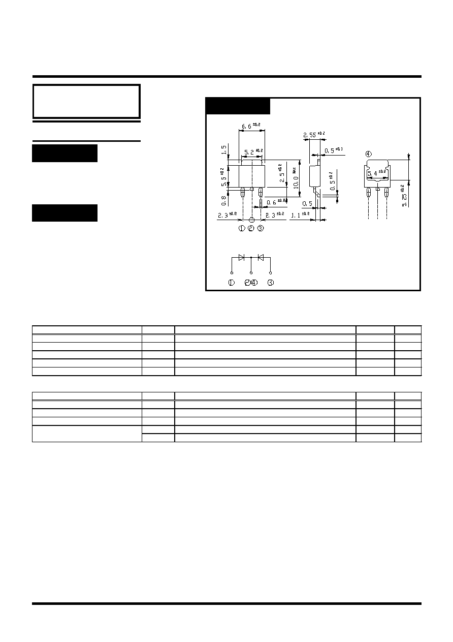
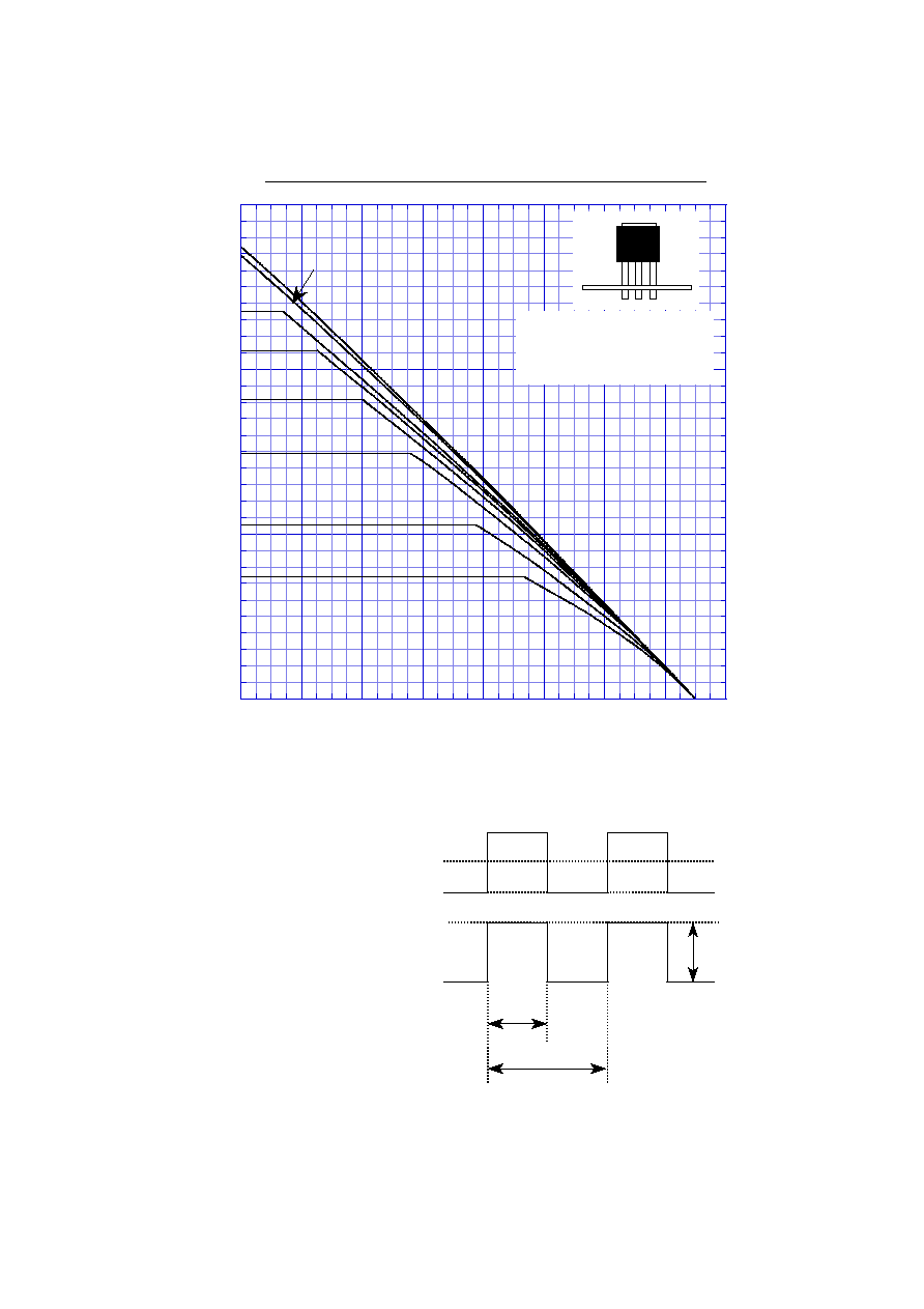
OUTLINE DIMENSIONS
OUTLINE DIMENSIONS
Unit : mm
Unit : mm
RATINGS
RATINGS
SHINDENGEN
SHINDENGEN
Case : E-pack
Case : E-pack
SMT
SMT
Low noise
Low noise
trr50ns
trr50ns
FEATURES
FEATURES
APPLICATION
APPLICATION
Switching power supply
Switching power supply
DC/DC converter
DC/DC converter
Free Wheel
Free Wheel
Home Appliances, Office Equipment
Home Appliances, Office Equipment
Telecommunication, Factory Automation
Telecommunication, Factory Automation
Dual
Dual
Super Fast Recovery Rectifiers
Super Fast Recovery Rectifiers
Absolute Maximum Ratings (If not specified Tc=25)
Item
Symbol
Conditions
Ratings
Unit
Storage Temperature
Tstg
-55150
Operating Junction Temperature
Tj
150
Maximum Reverse Voltage
V
RM
400
V
Average Rectified Forward Current
I
O
50Hz sine wave, R-load, Rating for each diode Io/2, Tc=61
5
A
Peak Surge Forward Current
I
FSM
50Hz sine wave, Non-repetitive 1 cycle peak value, Tj=25
50
A
Electrical Characteristics (If not specified Tc=25)
Item
Symbol
Conditions
Ratings
Unit
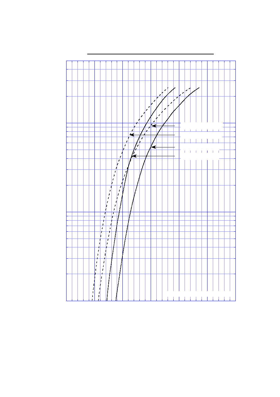
Forward Voltage
V
F
IF=2.5A,
Pulse measurement, Rating of per diode
Max.1.3
V
Reverse Current
I
R
V
R
=V
RM
, Pulse measurement, Rating of per diode
Max.10
A
Reverse Recovery Time
trr
I
F
=0.5A, I
R
=1A, Rating of per diode
Max.50
ns
Thermal Resistance
jc
junction to case
Max.12
/W
ja
junction to ambient
Max.55
/W
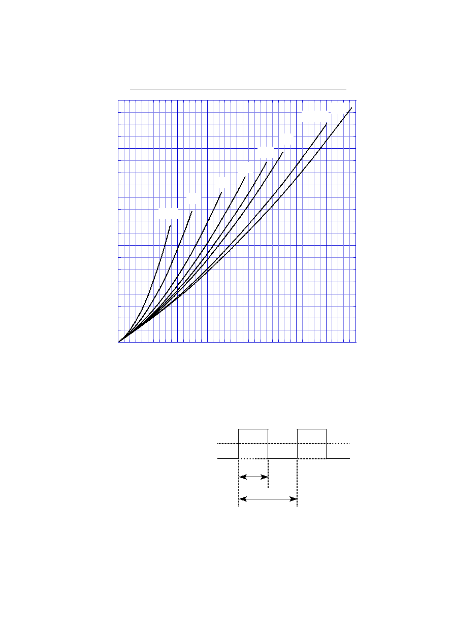
0
t
p
I
O
T
D=t
p
/T
0
2
4
6
8
10
0
1
2
3
4
5
6
7
8
DE5LC40
0.3
Forward Power Dissipation
Tj = 150
°
C
SIN
0.2
0.1
D=0.8
DC
0.5
0.05
Average Rectified Forward Current I
O
[A]
Forward Power Dissipation P
F
[W]
0
t
p
I
O
T
D=t
p
/T
0
0.5
1
1.5
2
2.5
3
0
20
40
60
80
100
120
140
160
DE5LC40
0.3
Derating Curve
SIN
0.2
0.1
D=0.8
DC
0.5
0.05
0
V
R
V
R
= V
RM
Ambient Temperature Ta [
°
C]
Average Rectified Forward Current I
O
[A]
Alumina substrate
Soldering land (leads) 1.5mm
×
2.5mm
Soldering land (heatsink) 7mm
Conductor layer 20
µ
m
Substrate thickness 0.64mm
0
t
p
I
O
T
D=t
p
/T
0
0.5
1
1.5
0
20
40
60
80
100
120
140
160
DE5LC40
0.3
Derating Curve
V
R
= V
RM
SIN
0.2
0.1
D=0.8
DC
0.5
0.05
0
V
R
Ambient Temperature Ta [
°
C]
Average Rectified Forward Current I
O
[A]
Glass-epoxy substrate
Soldering land 2mm
Lead length 9.5mm
Substrate thickness 1.6mm