 | –≠–ª–µ–∫—Ç—Ä–æ–Ω–Ω—ã–π –∫–æ–º–ø–æ–Ω–µ–Ω—Ç: BSM151 | –°–∫–∞—á–∞—Ç—å:  PDF PDF  ZIP ZIP |
Semiconductor Group
44
03.96
Type
Ordering Code
BSM 151
C67076-A1004-A2
Maximum Ratings
Parameter
Symbol
Values
Unit
Drain-source voltage
V
DS
500
V
Drain-gate voltage,
R
GS
= 20 k
V
DGR
500
Gate-source voltage
V
GS
±
20
Continuous drain current,
T
C
= 25 ∞C
I
D
48
A
Pulsed drain current,
T
C
= 25 ∞C
I
D puls
192
Operating and storage temperature range
T
j
,
T
stg
≠ 55 ... + 150
∞C
Power dissipation,
T
C
= 25 ∞C
P
tot
625
W
Thermal resistance
Chip-case
R
th JC
0.20
K/W
Insulation test voltage
2)
,
t
= 1 min.
V
is
2500
V
ac
Creepage distance, drain-source
≠
16
mm
Clearance, drain-source
≠
11
DIN humidity category, DIN 40 040
≠
F
≠
IEC climatic category, DIN IEC 68-1
≠
55/150/56
1)
See chapter Package Outline and Circuit Diagrams.
2)
Insulation test voltage between drain and base plate referred to standard climate 23/50 in acc. with
DIN 50 014, IEC 146, para. 492.1.
SIMOPAC
Æ
Module
BSM 151
V
DS
= 500 V
I
D
= 48 A
R
DS(on)
= 0.12
q
Power module
q
Single switch
q
N channel
q
Enhancement mode
q
Package with insulated metal base plate
q
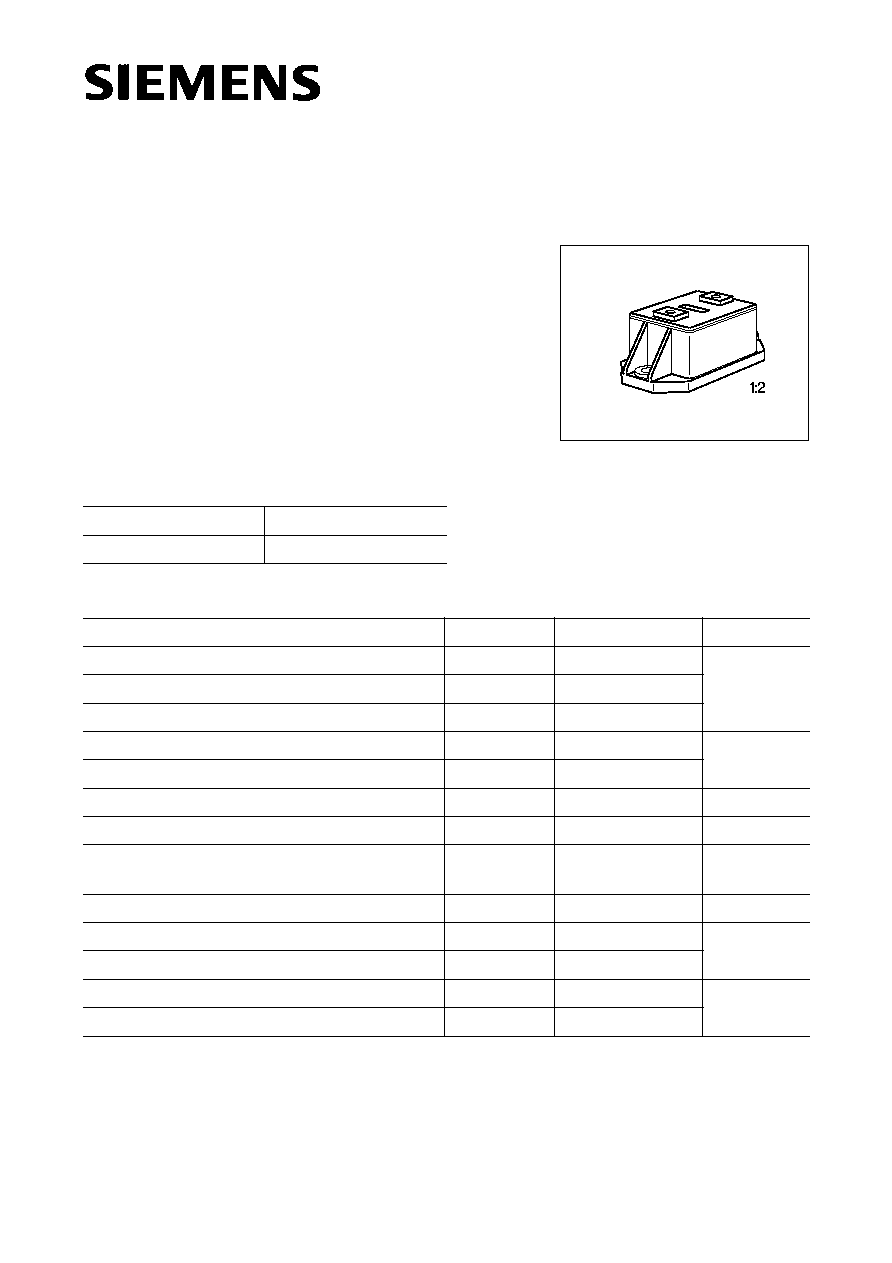
Package outline/Circuit diagram: 1
1)

Semiconductor Group
45
BSM 151
Electrical Characteristics
at
T
j
= 25 ∞C, unless otherwise specified.
Parameter
Symbol
Values
Unit
min.
typ.
max.
Static Characteristics
Drain-source breakdown voltage
V
GS
= 0,
I
D
= 0.25 mA
V
(BR)DSS
500
≠
≠
V
Gate threshold voltage
V
DS
=
V
GS
,
I
D
= 1 mA
V
GS(th)
2.1
3.0
4.0
Zero gate voltage drain current
V
DS
= 500 V,
V
GS
= 0
T
j
= 25 ∞C
T
j
= 125 ∞C
I
DSS
≠
≠
50
300
250
1000
µ
A
Gate-source leakage current
V
GS
= 20 V,
V
DS
= 0
I
GSS
≠
10
100
nA
Drain-source on-state resistance
V
GS
= 10 V,
I
D
= 30 A
R
DS(on)
≠
0.1
0.12
Dynamic Characteristics
Forward transconductance
V
DS
2
◊
I
D
◊
R
DS(on)max.
,
I
D
= 30 A
g
fs
30
45
≠
S
Input capacitance
V
GS
= 0,
V
DS
= 25 V,
f
= 1 MHz
C
iss
≠
8
11
nF
Output capacitance
V
GS
= 0,
V
DS
= 25 V,
f
= 1 MHz
C
oss
≠
1.2
1.7
Reverse transfer capacitance
V
GS
= 0,
V
DS
= 25 V,
f
= 1 MHz
C
rss
≠
0.5
0.7
Turn-on time
t
on
(
t
on
=
t
d (on)
+
t
r
)
V
CC
= 250 V,
V
GS
= 10 V
I
D
= 30 A,
R
GS
= 3.3
t
d (on)
≠
36
≠
ns
t
r
≠
25
≠
Turn-off time
t
off
(
t
off
=
t
d (off)
+
t
f
)
V
CC
= 250 V,
V
GS
= 10 V
I
D
= 30 A,
R
GS
= 3.3
t
d (off)
≠
260
≠
t
f
≠
50
≠

Semiconductor Group
46
Electrical Characteristics (cont'd)
at
T
j
= 25 ∞C, unless otherwise specified.
Parameter
Symbol
Values
Unit
min.
typ.
max.
Reverse diode
Continuous reverse drain current
T
C
= 25 ∞C
I
S
≠
≠
48
A
Pulsed reverse drain current
T
C
= 25 ∞C
I
SM
≠
≠
192
Diode forward on-voltage
I
F
= 96 A ,
V
GS
= 0
V
SD
≠
1.1
1.4
V
BSM 151

Semiconductor Group
47
Characteristics at
T
j
= 25 ∞C, unless otherwise specified.
Power dissipation
P
tot
=
f
(
T
C
)
parameter:
T
j
= 150 ∞C
Typ. transfer characteristic
I
D
=
f
(
V
GS
)
parameter:
t
p
= 80
µ
s,
V
DS
= 25 V
Typ. output characteristics
I
D
=
f
(
V
DS
)
parameter:
t
p
= 80
µ
s
Drain current
I
D
=
f
(
T
C
)
parameter:
V
GS
10 V,
T
j
= 150 ∞C
BSM 151

Semiconductor Group
48
Drain-source breakdown voltage
V
(BR)DSS
(
T
j
)
=
b
◊
V
(BR)DSS
(25 ∞C)
Typ. capacitances
C
=
f
(
V
DS
)
parameter:
V
GS
= 0,
f
= 1 MHz
Drain source on-resistance
R
DS (on)
=
f
(
T
j
)
parameter:
I
D
= 30 A;
V
GS
= 10 V, (spread)
Forward characteristics of reverse diode
I
F
=
f
(
V
SD
), parameter:
T
j
,
t
p
= 80
µ
s (spread)
BSM 151

Semiconductor Group
49
BSM 151
Typ. gate charge
V
GS
=
f
(
Q
Gate
)
parameter:
I
Dpuls
= 63 A
Safe operating area
I
D
=
f
(
V
DS
)
parameter: single pulse,
T
C
= 25 ∞C,
T
j
150 ∞C