
Semiconductor Group
04 / 1998
1
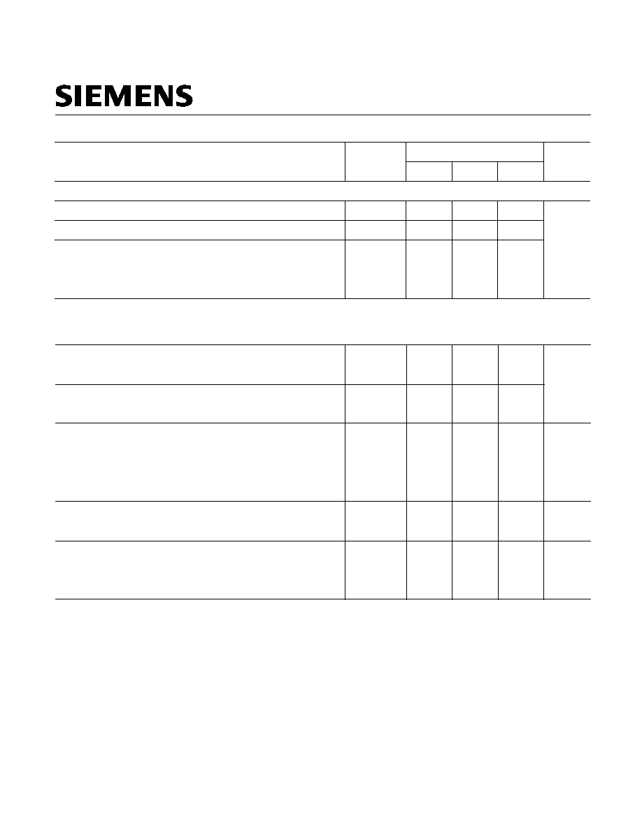
BSP 171 P
Preliminary data
SIPMOS
Æ
Power Transistor
∑
P-Channel
∑
Enhancement mode
∑
Avalanche rated
∑
Logic Level
∑
dv/dt rated
Pin 1
Pin2/4
Pin 3
G
D
S
Type
V
DS
I
D
R
DS(on)
@ V
GS
Package
Ordering Code
BSP 171 P
-60 V
-1.8 A 0.3
V
GS
= -10 V P-SOT223-4-1
-
Q67041-S4019
-
Continuous drain current
T
A
= 25 ∞C
T
A
= 100 ∞C
I
D
-1.8
-1.15
A
-7.2
Pulsed drain current
T
A
= 25 ∞C
I
D puls
mJ
Avalanche energy, single pulse
I
D
= -1.8 A, V
DD
= -25 V, R
GS
= 25
70
E
AS
Avalanche current,periodic limited by T
jmax
I
AR
A
-1.8
0.18
mJ
Avalanche energy,periodic limited by T
j(max)
E
AR
KV/µs
dv/dt
Reverse diode dv/dt
I
S
= -1.8 A, V
DD
V
(BR)DSS
, di/dt = 100 A/µs,
T
jmax
= 150 ∞C
6
Gate source voltage
V
GS
±
14
V
1.8
W
Power dissipation, T
A
= 25 ∞C
P
tot
∞C
Operating temperature
-55 ...+150
T
j
Storage temperature
T
stg
-55 ...+150
55/150/56
IEC climatic category; DIN IEC 68-1
Maximum Ratings, at Tj = 25 ∞C, unless otherwise specified
Value
Unit
Parameter
Symbol
Semiconductor Group
04 / 1998
2
BSP 171 P
Preliminary data
Electrical Characteristics
Unit
Values
Symbol
Parameter
at Tj = 25 ∞C, unless otherwise specified
typ.
max.
min.
Thermal Characteristics
tbd
-
R
thJS
Thermal resistance,
junction -soldering point (Pin 4)
K/W
tbd
-
Thermal resistance, junction - ambient
R
thJA
-
-
-
70
SMD version, device on PCB:
@ min. footprint
@ 6 cm
2
cooling area
F)
-
-
R
thJA
tbd
tbd
Static Characteristics
-
-
-60
V
(BR)DSS
Drain- source breakdown voltage
V
GS
= 0 V, I
D
= -0.25 mA
V
-1
-1.5
V
GS(th)
Gate threshold voltage, V
GS
= V
DS
I
D
= -460 µA, T
j
= 25 ∞C
-2
-
-
-
-
-0.1
-
µA
Zero gate voltage drain current
V
DS
= -60 V, V
GS
= 0 V, T
j
= -40 ∞C
V
DS
= -60 V, V
GS
= 0 V, T
j
= 25 ∞C
V
DS
= -60 V, V
GS
= 0 V, T
j
= 150 ∞C
I
DSS
-0.1
-1
-100
-10
-100
nA
-
I
GSS
Gate-source leakage current
V
GS
= -20 V, V
DS
= 0 V
0.3
0.21
Drain-Source on-state resistance
V
GS
= -4.5 V, I
D
= -1.5 A
V
GS
= -10 V, I
D
= -1.8 A
R
DS(on)
0.45
0.3
-
-

Semiconductor Group
04 / 1998
4
BSP 171 P
Preliminary data
Electrical Characteristics
Parameter
Symbol
Values
Unit
at Tj = 25 ∞C, unless otherwise specified
min.
typ.
max.
Dynamic Characteristics
Gate charge at threshold
V
DD
= -24 V, I
D
-0,1 A, V
GS
= 0 to - 1 V
Q
G(th)
-
0.6
0.9
nC
Gate charge at V
gs
=5V
V
DD
= -24 V, I
D
= -1.8 A , V
GS
= 0 to -5 V
Qg(5)
-
8
12
Gate charge total
V
DD
= -24 V, I
D
= -1.8 A, V
GS
= 0 to -10 V
Q
g
-
14
21
nC
Gate plateau voltage
V
DD
= -24 V, I
D
= -1.8 A
V
(plateau)
-
2.8
-
V
Reverse Diode
-1.8
A
-
-
I
S
Inverse diode continuous forward current
T
A
= 25 ∞C
-7.2
Inverse diode direct current,pulsed
T
A
= 25 ∞C
-
I
SM
-
-1.2
V
-0.95
Inverse diode forward voltage
V
GS
= 0 V, I
F
= -3.6 A
-
V
SD
150
Reverse recovery time
V
R
= -30 V, I
F
=I
S
, di
F
/dt = 100 A/µs
t
rr
ns
100
-
0.3
Reverse recovery charge
V
R
= -30 V, I
F=
l
S
, di
F
/dt = 100 A/µs
-
Q
rr
µC
0.2

Semiconductor Group
04 / 1998
5
BSP 171 P
Preliminary data
Edition 7.97
Published by Siemens AG,
Bereich Halbleiter Vetrieb,
Werbung, Balanstraþe 73,
81541 M¸nchen
© Siemens AG 1997
All Rights Reserved.
Attention please!
As far as patents or other rights of third parties are concerned, liability is only assumed for components,
not for applications, processes and circuits implemented within components or assemblies.
The information describes a type of component and shall not be considered as warranted characteristics.
Terms of delivery and rights to change design reserved.
For questions on technology, delivery and prices please contact the Semiconductor Group Offices in Germany
or the Siemens Companies and Representatives worldwide (see address list).
Due to technical requirements components may contain dangerous substances. For information on the types
in question please contact your nearest Siemens Office, Semiconductor Group.
Siemens AG is an approved CECC manufacturer.
Packing
Please use the recycling operators known to you. We can also help you - get in touch with your nearest sales
office. By agreement we will take packing material back, if it is sorted. You must bear the costs of transport.
For packing material that is returned to us unsorted or which we are not obliged to accept, we shall have to
invoice you for any costs incurred.
Components used in life-support devices or systems must be expressly authorized for such purpose!
Critical components
1
of the Semiconductor Group of Siemens AG, may only be used in life-support devices or
systems
2
with the express written approval of the Semiconductor Group of Siemens AG.
1)A critical component is a component used in a life-support device or system whose failure can reasonably be
expected to cause the failure of that life-support device or system, or to affect its safety or effectiveness of
that device or system.
2)Life support devices or systems are intended (a) to be implanted in the human body, or (b) to support and/or
maintain and sustain and/or protecf human life. If they fail, it is reasonable to assume that the health of the
