 | –≠–ª–µ–∫—Ç—Ä–æ–Ω–Ω—ã–π –∫–æ–º–ø–æ–Ω–µ–Ω—Ç: BTS542D2 | –°–∫–∞—á–∞—Ç—å:  PDF PDF  ZIP ZIP |
PROFETÆ BTS 542 D2
Semiconductor Group
Page 1 of 13
13.Nov.95
Smart Highside Power Switch
Features
∑
Overload protection
∑
Current limitation
∑
Short-circuit protection
∑
Thermal shutdown
∑
Overvoltage protection (including load dump)
∑
Fast demagnetization of inductive loads
∑
Reverse battery protection
1)
∑
Undervoltage and overvoltage shutdown with
auto-restart and hysteresis
∑
CMOS diagnostic output
∑
Open load detection in ON-state
∑
CMOS compatible input
∑
Loss of ground and loss of
V
bb
protection
2)
∑
Electrostatic discharge (ESD) protection
Application
∑
m
C compatible power switch with diagnostic
feedback for 12 V and 24 V DC grounded loads
∑
All types of resistive, inductive and capacitve loads
∑
Replaces electromechanical relays and discrete circuits
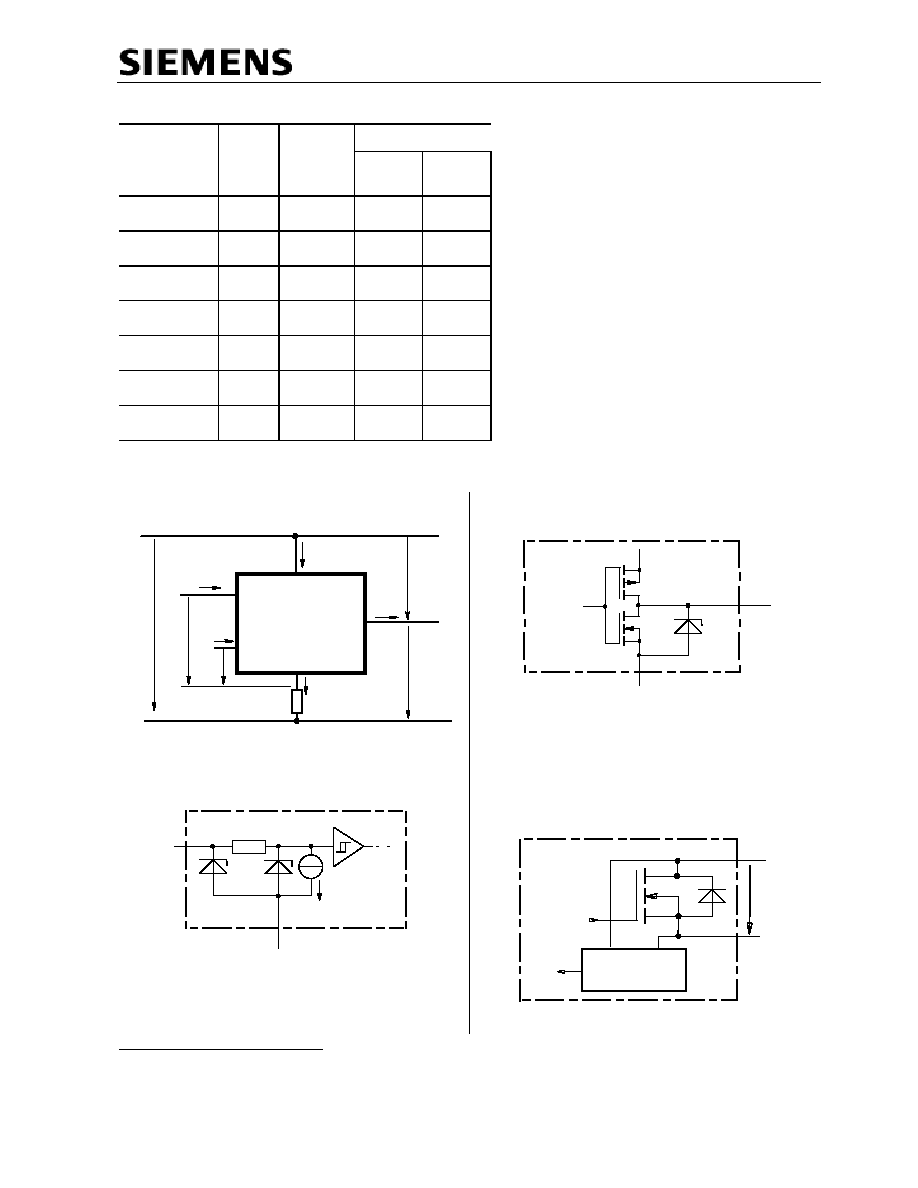
General Description
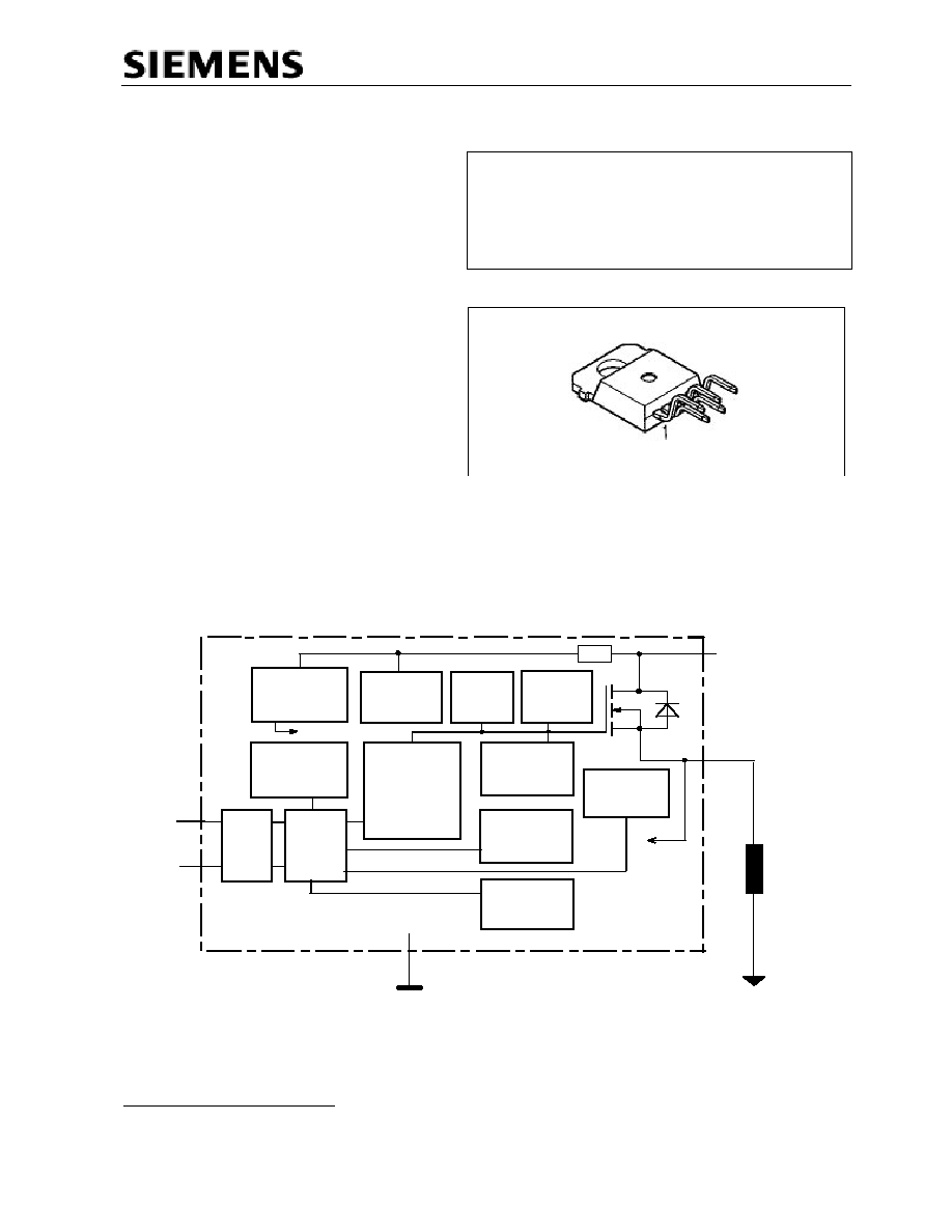
N channel vertical power FET with charge pump, ground referenced CMOS compatible input and diagnostic
feedback, integrated in Smart SIPMOS
‚
chip on chip technology. Fully protected by embedded protection
functions.
+ Vbb
IN
ST
Signal GND
ESD
PROFET
Æ
OUT
GND
Logic
Voltage
sensor
Voltage
source
Open load
detection
Short circuit
detection
Charge pump
Level shifter
Temperature
sensor
Rectifier
Limit for
unclamped
ind. loads
Gate
protection
Current
limit
2
4
1
3
5
Load GND
Load
8
Logic
Overvoltage
protection
Rbb
1)
No external components required, reverse load current limited by connected load.
2)
Additional external diode required for charged inductive loads
Product Summary
Overvoltage protection
V
bb(AZ)
63
V
Operating voltage
V
bb(on)
4.5 ... 42 V
On-state resistance
R
ON
18 m
W
Load current (ISO)
I
L(ISO)
21
A
Current limitation
I
L(SCr)
70
A
TO-218AB/5
5
Standard
BTS 542 D2
Semiconductor Group
Page 2
13.Nov.95
Pin
Symbol
Function
1
GND
-
Logic ground
2
IN
I
Input, activates the power switch in case of logical high signal
3
Vbb
+
Positive power supply voltage,
the tab is shorted to this pin
4
ST
S
Diagnostic feedback, low on failure
5
OUT
(Load, L)
O
Output to the load
Maximum Ratings at
T
j
= 25 ∞C unless otherwise specified
Parameter
Symbol
Values
Unit
Supply voltage (overvoltage protection see page 3)
V
bb
63
V
Load dump protection
V
LoadDump
=
U
A
+
V
s
,
U
A
= 13.5 V
R
I
= 2
W
,
R
L
= 1.1
W
,
t
d
= 200 ms, IN= low or high
V
Load dump
3
)
80
V
Load current (Short-circuit current, see page 4)
I
L
self-limited
A
Operating temperature range
Storage temperature range
T
j
T
stg
-40 ...+150
-55 ...+150
∞C
Power dissipation (DC)
P
tot
167
W
Inductive load switch-off energy dissipation,
single pulse
T
j
=150 ∞C:
E
AS
2.1
J
Electrostatic discharge capability (ESD)
(Human Body Model)
V
ESD
2.0
kV
Input voltage (DC)
V
IN
-0.5 ... +6
V
Current through input pin (DC)
Current through status pin (DC)
see internal circuit diagrams page 6...
I
IN
I
ST
±
5.0
±
5.0
mA
Thermal resistance
chip - case:
junction - ambient (free air):
R
thJC
R
thJA
£
0.75
£
45
K/W
3)
V
Load dump
is setup without the DUT connected to the generator per ISO 7637-1 and DIN 40839
BTS 542 D2
Semiconductor Group
Page 3
13.Nov.95
Electrical Characteristics
Parameter and Conditions
Symbol
Values
Unit
at
T
j
= 25 ∞C,
V
bb
= 12 V unless otherwise specified
min
typ
max
Load Switching Capabilities and Characteristics
On-state resistance (pin 3 to 5)
I
L
= 5 A
T
j
=25 ∞C:
T
j
=150 ∞C:
R
ON
--
15
28
18
35
m
W
Nominal load current (pin 3 to 5)
ISO Proposal:
V
ON
= 0.5 V,
T
C
= 85 ∞C
I
L(ISO)
17
21
--
A
Output current (pin
5
) while GND disconnected or
GND pulled up,
V
IN
= 0, see diagram page 7,
T
j
=-40...+150∞C
I
L(GNDhigh)
--
--
1
mA
Turn-on time
to 90%
V
OUT
:
Turn-off time
to 10%
V
OUT
:
R
L
= 12
W
,
T
j
=-40...+150∞C
t
on
t
off
100
10
--
--
350
130
m
s
Slew rate on
10 to 30%
V
OUT
,
R
L
= 12
W
,
T
j
=-40...+150∞C
d
V /dt
on
0.2
--
2
V/
m
s
Slew rate off
70 to 40%
V
OUT
,
R
L
= 12
W
,
T
j
=-40...+150∞C
-d
V/dt
off
0.4
--
5
V/
m
s
Operating Parameters
Operating voltage
4
)
T
j
=-40...+150∞C:
V
bb(on)
4.5
--
42
V
Undervoltage shutdown
T
j
=-40...+150∞C:
V
bb(under)
2.4
--
4.5
V
Undervoltage restart
T
j
=-40...+150∞C:
V
bb(u rst)
--
--
4.5
V
Undervoltage restart of charge pump
see diagram page 12
T
j
=-40...+150∞C:
V
bb(ucp)
--
6.5
7.5
V
Undervoltage hysteresis
D
V
bb(under)
=
V
bb(u rst)
-
V
bb(under)
D
V
bb(under)
--
0.2
--
V
Overvoltage shutdown
T
j
=-40...+150∞C:
V
bb(over)
42
--
52
V
Overvoltage restart
T
j
=-40...+150∞C:
V
bb(o rst)
42
--
--
V
Overvoltage hysteresis
T
j
=-40...+150∞C:
D
V
bb(over)
--
0.2
--
V
Overvoltage protection
5
)
T
j
=-40∞C:
I
bb
=40 mA
T
j
=25...+150∞C:
V
bb(AZ)
60
63
--
67
--
V
Standby current (pin 3)
T
j
=-40...+25∞C
:
V
IN
=0, I
ST
=0
,
T
j
=150∞C:
I
bb(off)
--
--
12
18
25
60
m
A
Leakage output current (included in
I
bb(off)
)
V
IN
=0
I
L(off)
--
6
--
m
A
Operating current (Pin 1)
6)
,
V
IN
=5 V
I
GND
--
1.1
--
mA
4
)
At supply voltage increase up to
V
bb
= 6.5 V typ without charge pump,
V
OUT
ª
V
bb
- 2 V
5)
see also
V
ON(CL)
in table of protection functions and circuit diagram page 7. Meassured without load
.
6
)
Add
I
ST
, if
I
ST
> 0, add
I
IN
, if
V
IN
>5.5 V

BTS 542 D2
Parameter and Conditions
Symbol
Values
Unit
at
T
j
= 25 ∞C,
V
bb
= 12 V unless otherwise specified
min
typ
max
Semiconductor Group
Page 4
13.Nov.95
Protection Functions
Initial peak short circuit current limit (pin 3 to 5)
7
)
,
(
max 400
m
s if
V
ON
>
V
ON(SC)
)
I
L(SCp)
T
j
=-40∞C:
T
j
=25∞C:
T
j
=+150∞C:
--
--
45
--
95
--
140
--
--
A
Repetitive short circuit current limit
I
L(SCr)
T
j
=
T
jt
(see timing diagrams, page 10)
30
70
--
A
Short circuit shutdown delay after input pos. slope
V
ON
>
V
ON(SC)
,
T
j
=-40..+150∞C:
min value valid only, if input "low" time exceeds 30
m
s
t
d(SC)
80
--
400
m
s
Output clamp (inductive load switch off)
at
V
OUT
=
V
bb
-
V
ON(CL),
I
L
= 30 mA
V
ON(CL)
--
58
--
V
Short circuit shutdown detection voltage
(pin 3 to 5)
V
ON(SC)
--
8.3
--
V
Thermal overload trip temperature
T
jt
150
--
--
∞C
Thermal hysteresis
,
T
jt
--
10
--
K
Inductive load switch-off energy dissipation
8)
,
T
j Start
= 150 ∞C, single pulse
V
bb
= 12 V:
V
bb
= 24 V:
E
AS
E
Load12
E
Load24
--
--
2.1
1.7
1.2
J
Reverse battery (pin 3 to 1)
9
)
-
V
bb
--
--
32
V
Integrated resistor in
V
bb
line
R
bb
--
120
--
W
Diagnostic Characteristics
Open load detection current
T
j
=-40 ∞C
:
(on-condition)
T
j
=25..150∞C:
I
L (OL)
2
2
--
--
1900
1500
mA
7
)
Short circuit current limit for max. duration of t
d(SC) max
=400
m
s, prior to shutdown
8)
While demagnetizing load inductance, dissipated energy in PROFET is
E
AS
=
Ú
Ú
V
ON(CL)
*
i
L
(t) dt, approx.
E
AS
=
1
/
2
* L * I
2
L
* (
V
ON(CL)
V
ON(CL)
-
V
bb
), see diagram page 8
9
)
Reverse load current (through intrinsic drain-source diode) is normally limited by the connected load.
Reverse current I
GND
of
ª
0.3 A at V
bb
= -32 V through the logic heats up the device. Time allowed under
these condition is dependent on the size of the heatsink. Reverse I
GND
can be reduced by an additional
external GND-resistor (150
W
). Input and Status currents have to be limited (see max. ratings page 2 and
circuit page 7).
BTS 542 D2
Parameter and Conditions
Symbol
Values
Unit
at
T
j
= 25 ∞C,
V
bb
= 12 V unless otherwise specified
min
typ
max
Semiconductor Group
Page 5
13.Nov.95
Input and Status Feedback
10
)
Input turn-on threshold voltage
T
j
=-40..+150∞C:
V
IN(T+)
1.5
--
2.4
V
Input turn-off threshold voltage
T
j
=-40..+150∞C:
V
IN(T-)
1.0
--
--
V
Input threshold hysteresis
D
V
IN(T)
--
0.5
--
V
Off state input current (pin 2),
V
IN
= 0.4 V
I
IN(off)
1
--
30
m
A
On state input current (pin 2),
V
IN
= 3.5 V
I
IN(on)
10
25
50
m
A
Status invalid after positive input slope
(short circuit)
Tj=-40 ... +150∞C:
t
d(ST SC)
80
200
400
m
s
Status invalid after positive input slope
(open load)
Tj=-40 ... +150∞C:
t
d(ST)
350
--
1600
m
s
Status output (CMOS)
T
j
=-40...+150∞C,
I
ST
= - 50
m
A:
T
j
=-40...+150∞C,
I
ST
= +1.6 mA:
Max. status current for
current source
(out):
valid status output,
current sink
(in) :
T
j
=-40...+150∞C
V
ST(high)
11
)
V
ST(low)
-I
ST
+I
ST
12)
4.4
--
--
--
5.1
--
--
--
6.5
0.4
0.25
1.6
V
mA
10)
If a ground resistor R
GND
is used, add the voltage drop across this resistor.
11
) V
St high
ª
V
bb
during undervoltage shutdown
12
) No current sink capability during undervoltage shutdown
BTS 542 D2
Semiconductor Group
Page 6
13.Nov.95
Truth Table
Input-
Output
Status
level
level
542
D2
542
E2
Normal
operation
L
H
L
H
H
H
H
H
Open load
L
H
13)
H
H
L
H
L
Short circuit
to GND
L
H
L
L
H
L
H
L
Short circuit
to V
bb
L
H
H
H
H
H (L
14)
)
H
H (L
14)
)
Overtem-
perature
L
H
L
L
L
L
L
L
Under-
voltage
L
H
L
L
L
15)
L
15)
H
H
Overvoltage
L
H
L
L
L
L
H
H
L = "Low" Level
H = "High" Level
13
) Power Transistor off, high impedance
14
) Low resistance short V
bb
to output may be detected by no-load-detection
15
) No current sink capability during undervoltage shutdown
Terms
PROFET
V
IN
ST
OUT
GND
bb
VST
VIN
IST
IIN
Vbb
Ibb
IL
VOUT
IGND
VON
1
2
4
3
5
R GND
Input circuit (ESD protection)
IN
GND
I
R
ZD
ZD
II
I1
I2
ESD-
ZD
I1
6.1 V typ., ESD zener diodes are not to be used
as voltage clamp at DC conditions. Operation in this
mode may result in a drift of the zener voltage
(increase of up to 1 V).
Status output
ST
8
Logic
GND
ESD-
ZD
Zener diode: 6.1 V typ., max 5 mA, V
Logic
5 V typ,
ESD zener diodes are not to be used as voltage clamp
at DC conditions. Operation in this mode may result in
a drift of the zener voltage (increase of up to 1 V).
Short Circuit detection
Fault Condition:
V
ON
> 8.3 V typ.; IN high
Short circuit
detection
Logic
unit
+ Vbb
OUT
V
ON
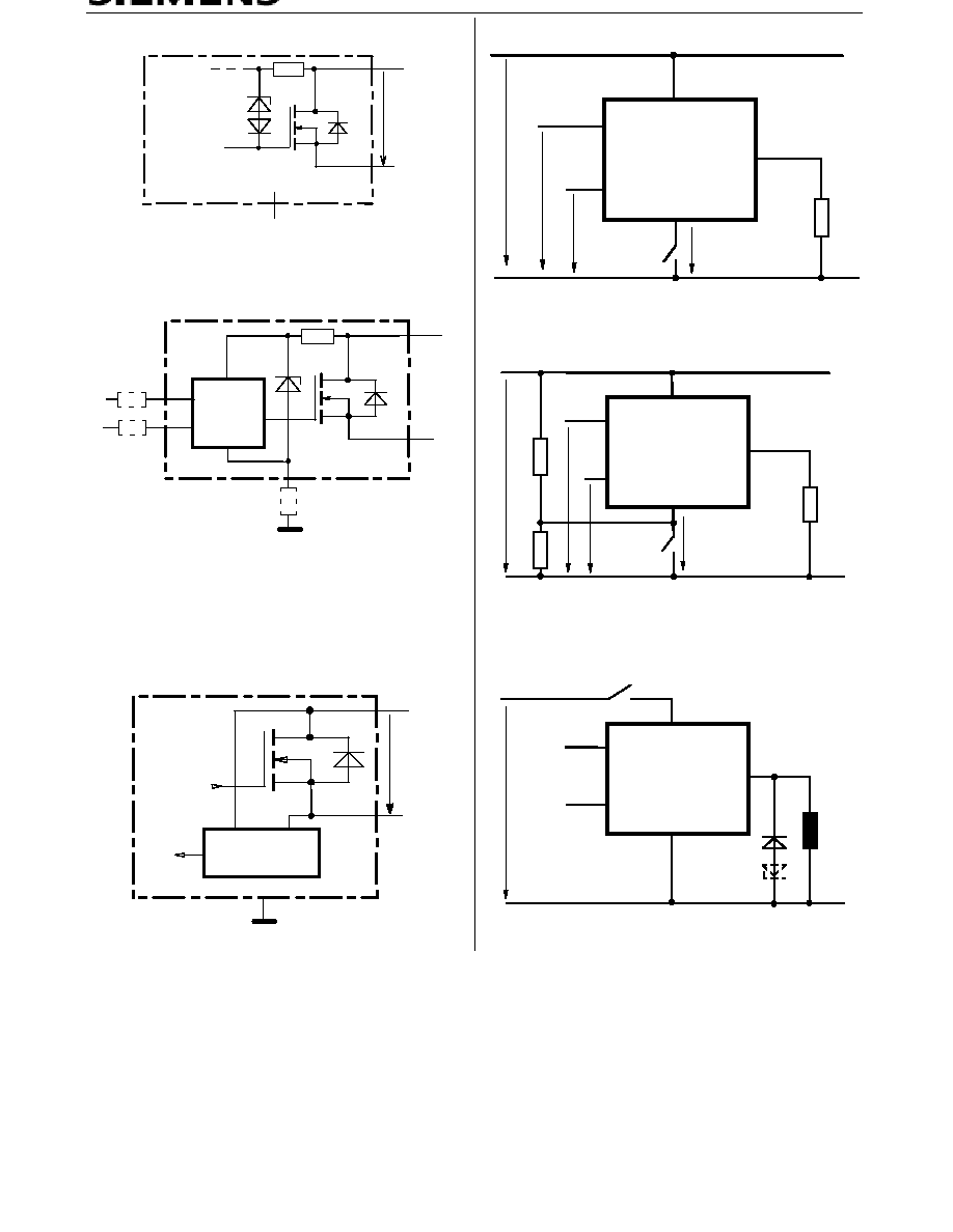
BTS 542 D2
Semiconductor Group
Page 7
13.Nov.95
Inductive and overvoltage output clamp
+ Vbb
OUT
GND
VZ
VON
V
ON
clamped to 58 V typ.
Overvolt. and reverse batt. protection
+ Vbb
VOUT
IN
ST
bb
R
Signal GND
Logic
PROFET
VZ
R
GND
GND
IN
R
ST
R
R
bb
= 120
W
typ
.
,
V
Z
+
R
bb
*40 mA = 67 V typ., add
R
GND
, R
IN
, R
ST
for extended protection
Open-load detection
ON-state diagnostic condition:
V
ON
<
R
ON
*
I
L(OL)
; IN
high
Open load
detection
Logic
unit
+ Vbb
OUT
ON
V
ON
GND disconnect
PROFET
V
IN
ST
OUT
GND
bb
Vbb
1
2
4
3
5
VIN VST
VGND
Any kind of load. In case of Input=high is
V
OUT
ª
V
IN
-
V
IN(T+)
.
Due to V
GND
>0, no V
ST
= low signal available.
GND disconnect with GND pull up
PROFET
V
IN
ST
OUT
GND
bb
Vbb
1
2
4
3
5
VGND
VIN VST
Any kind of load. If V
GND >
V
IN
-
V
IN(T+)
device stays off
Due to V
GND
>0, no V
ST
= low signal available.
V
bb
disconnect with charged inductive
load
PROFET
V
IN
ST
OUT
GND
bb
Vbb
1
2
4
3
5
high
BTS 542 D2
Semiconductor Group
Page 8
13.Nov.95
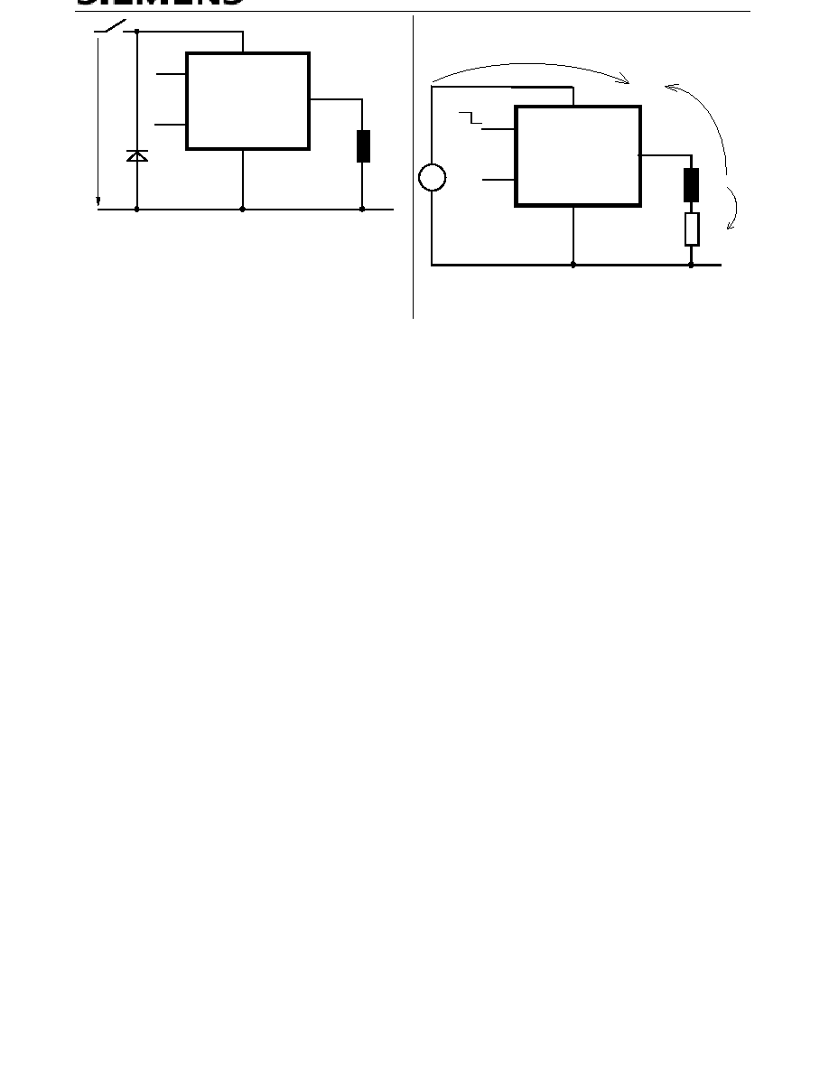
PROFET
V
IN
ST
OUT
GND
bb
Vbb
1
2
4
3
5
high
Inductive Load switch-off energy
dissipation
PROFET
V
IN
ST
OUT
GND
bb
=
E
E
E
EAS
bb
L
R
ELoad
Energy dissipated in PROFET E
AS
= E
bb
+ E
L
- E
R
.
E
Load
<
E
L
,
E
L
=
1/2
*
L * I
2
L
BTS 542 D2
Semiconductor Group
Page 9
13.Nov.95
Options Overview
all versions: High-side switch, Input protection, ESD protection, load dump and
reverse battery protection , protection against loss of ground
Type
BTS 542D2 542E2
Logic version
D
E
Overtemperature protection
Tj >150 ∞C, latch function
16)17)
Tj >150 ∞C, with auto-restart on cooling
X
X
Short-circuit to GND protection
switches off when
V
ON
>8.3 V typ.
16)
(when first turned on after approx. 200
m
s)
X
X
Open load detection
in OFF-state with sensing current 30
m
A typ.
in ON-state with sensing voltage drop across
power transistor
X
X
Undervoltage shutdown with auto restart
X
X
Overvoltage shutdown with auto restart
X
X
Status feedback for
overtemperature
short circuit to GND
short to V
bb
open load
undervoltage
overvoltage
X
X
-
18)
X
X
X
X
X
-
18)
X
-
-
Status output type
CMOS
Open drain
X
X
Output negative voltage transient limit
(fast inductive load switch off)
to
V
bb
-
V
ON(CL)
X
X
Load current limit
high level
(can handle loads with high inrush currents)
medium level
low level
(better protection of application)
X
X
16
) Latch except when V
bb
-
V
OUT
<
V
ON(SC)
after shutdown. In most cases
V
OUT
= 0 V after shutdown (
V
OUT
π
0 V only if forced externally). So the device remains latched unless
V
bb
<
V
ON(SC)
(see page 4). No latch
between turn on and t
d(SC)
.
17)
With latch function. Reseted by a) Input low, b) Undervoltage, c) Overvoltage
18
) Low resistance short V
bb
to output may be detected by no-load-detection
BTS 542 D2
Semiconductor Group
Page 10
13.Nov.95
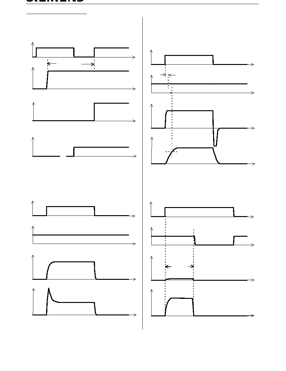
Timing diagrams
Figure 1a: V
bb
turn on:
AAA
AAA
A
A
AAAA
AAAA
AA
AA
AA
AA
AAA
AAA
AAA
AAA
AAA
AAA
AAA
AAAA
AAAA
AAAA
AAAA
AAAA
AAAA
AAA
AAA
A
A
AAAA
AAAA
AAA
AAA
AAAA
AAAA
AAA
AAA
AAAA
AAAA
AAAA
AAAA
A
A
A
A
AAAA
AAAA
AAA
AAA
A
A
AAAA
AAAA
AAA
AAA
AAA
AAA
A
AAAA
AAAA
AA
AA
AA
AA
AAA
AAA
AAA
AAA
AAA
AAA
AAA
AAA
AAA
AAA
AAA
AAAAAAAAAAAAAAA
AA
AA
AA
AA
AA
AA
AA
AA
AA
AA
AA
AAAA
AAAA
AAA
AAA
AAAA
AAAA
AAA
AAA
AA
AA
AA
AA
AA
AA
AA
AA
AA
AA
AA
AAAAAAAAA
A
AAAAAAA
A
AAAAAAA
IN
V
OUT
t
V
ST CMOS
bb
A
A
t
d(bb IN)
in case of too early
V
IN=high the device may not turn on (curve A)
t
d(bb IN)
approx. 150
m
s
Figure 2a: Switching a lamp,
IN
ST
OUT
L
t
V
I
Figure 2b: Switching an inductive load
AA
AA
AA
AA
AA
AA
AA
AA
AA
AA
AA
AA
AA
AA
IN
ST
L
t
V
I
*)
OUT
t
d(ST)
I
L(OL)
*) if the time constant of load is too large, open-load-status may occur
Figure 3a: Turn on into short circuit,
IN
ST
OUT
L
t
V
I
td(SC)
td(SC) approx. 200
m
s if
V
bb
-
V
OUT
> 8.3 V typ.
BTS 542 D2
Semiconductor Group
Page 11
13.Nov.95
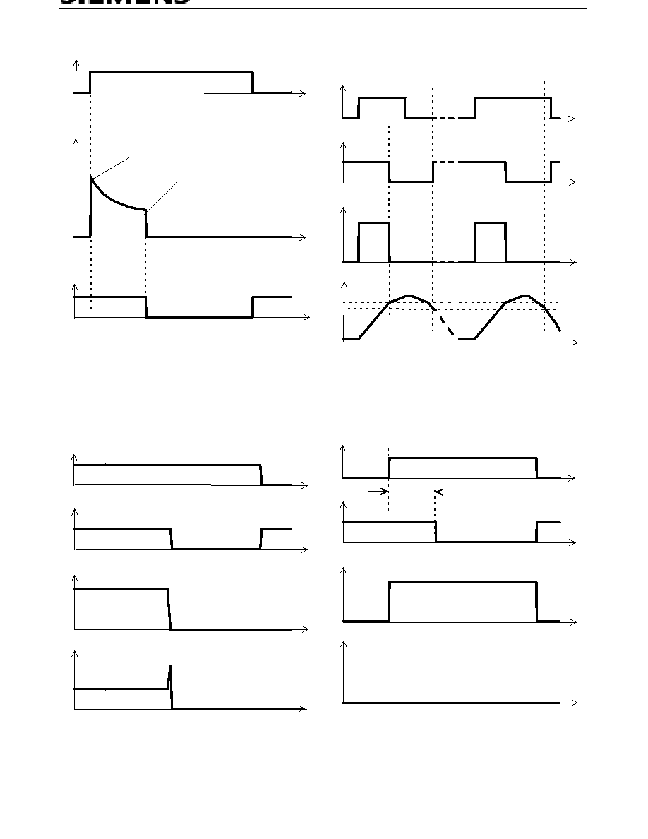
Figure 3b: Turn on into overload,
IN
ST
L
t
I
L(SCr)
I
L(SCp)
I
Heating up may require several milliseconds,
V
bb
-
V
OUT
< 8.3 V typ.
,
V
bb
-
V
OUT
< 8.3 V typ.
Figure 3c: Short circuit while on:
IN
ST
OUT
L
t
V
I
**)
**) current peak approx. 20
m
s
Figure 4a: Overtemperature,
Reset if (IN=low) and (
T
j
<
T
jt
)
IN
ST
OUT
J
t
V
T
*) ST goes high , when
V
IN=low and
T
j<
T
jt
Figure 5a: Open load: detection in ON-state, turn
on/off to open load
IN
ST
OUT
L
t
V
I
open
t
d(ST)

BTS 542 D2
Semiconductor Group
Page 12
13.Nov.95
Figure 5b: Open load: detection in ON-state, open
load occurs in on-state
IN
ST
OUT
L
t
V
I
open
normal
normal
t
d(ST OL1)
t
d(ST OL2)
t
d(ST OL1)
= tbd
m
s typ., t
d(ST OL2)
= tbd
m
s typ
Figure 6a: Undervoltage:
IN
V
OUT
t
V
bb
ST CMOS
V
V
bb(under)
bb(u rst)
bb(u cp)
8
Figure 6b: Undervoltage restart of charge pump
V
ON
[V]
bb(under)
V
V
bb(u rst)
V
bb(over)
V
bb(o rst)
V
bb(u cp)
off
on
off
V
ON(CL)
V
bb
V
on
V
bb
[V]
charge pump starts at
V
bb(ucp)
=6.5 V typ.
Figure 7a: Overvoltage:
IN
V
OUT
t
V
bb
ST
ON(CL)
V
V
bb(over)
V
bb(o rst)
BTS 542 D2
Semiconductor Group
Page 13
13.Nov.95
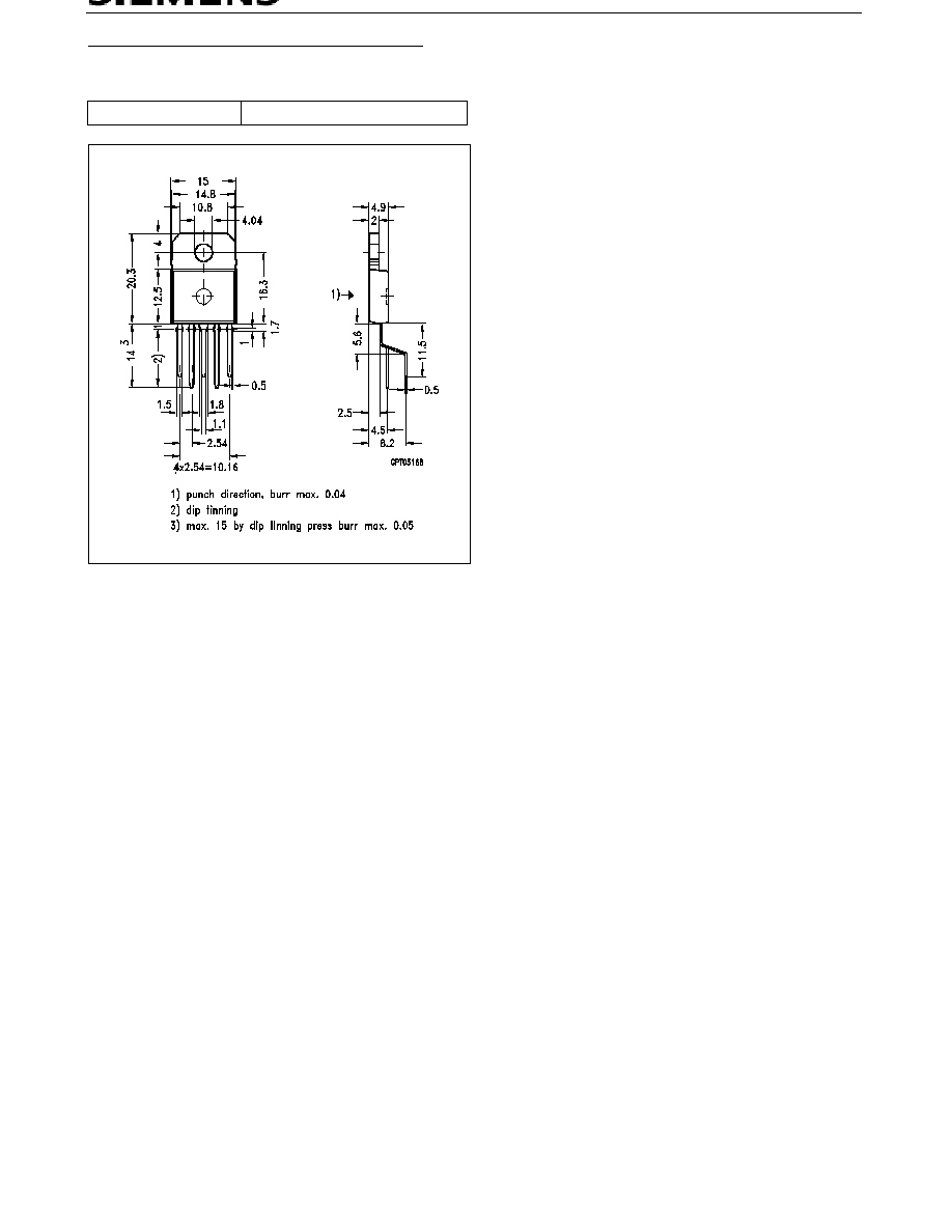
Package and Ordering Code
All dimensions in mm
Standard TO-218AB/5
Ordering code
BTS 542 D2
Q67060-S6950-A2