 | –≠–ª–µ–∫—Ç—Ä–æ–Ω–Ω—ã–π –∫–æ–º–ø–æ–Ω–µ–Ω—Ç: BTS555 | –°–∫–∞—á–∞—Ç—å:  PDF PDF  ZIP ZIP |
PROFETÆ Target Data Sheet BTS555
Semiconductor Group Page 1 of 16
1998-Jan-14
Smart Highside High Current Power Switch
Features
∑
Overload protection
∑
Current limitation
∑
Short circuit protection
∑
Overtemperature protection
∑
Overvoltage protection (including load dump)
∑
Clamp of negative voltage at output
∑
Fast deenergizing of inductive loads
1)
∑
Low ohmic inverse current operation
∑
Reverse battery protection
∑
Diagnostic feedback with load current sense
∑
Open load detection via current sense
∑
Loss of
V
bb
protection
2)
∑
Electrostatic discharge (ESD) protection
Application
∑
Power switch with current sense diagnostic
feedback for 12
V and 24
V DC grounded loads
∑
Most suitable for loads with high inrush current
like lamps and motors; all types of resistive and
inductive loads
∑
Replaces electromechanical relays, fuses and discrete circuits
General Description
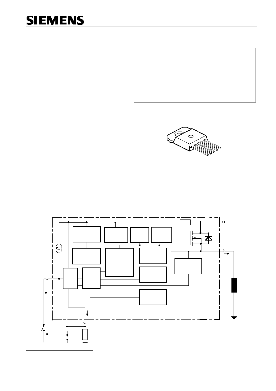
N channel vertical power FET with charge pump, current controlled input and diagnostic feedback with load
current sense, integrated in Smart SIPMOS
Æ
chip on chip technology. Fully protected by embedded protection
functions.
IN
Charge pump
Level shifter
Rectifier
Limit for
unclamped
ind. loads
Gate
protection
Current
limit
2
Overvoltage
protection
+ Vbb
PROFET
Æ
OUT
3 & Tab
1, 5
Load GND
Load
Output
Voltage
detection
R
IS
IS
4
I
IS
I
L
V
IS
I
IN
Logic GND
Voltage
sensor
Voltage
source
Current
Sense
Logic
ESD
Temperature
sensor
R
bb
V
IN
1
)
With additional external diode.
2)
Additional external diode required for energized inductive loads (see page 9).
Product Summary
Overvoltage protection
V
bb(AZ)
63
V
Output clamp
V
ON(CL)
42
V
Operating voltage
V
bb(on)
5.0
...
34
V
On-state resistance
R
ON
2.9
m
Load current (ISO)
I
L(ISO)
132
A
Short circuit current limitation
I
L(SCp)
400
A
Current sense ratio
I
L :
I
IS
25 000
TO-218AB/5
5
1
Straight leads
Target Data Sheet BTS555
Semiconductor Group
Page 2
1998-Jan-14
Pin
Symbol
Function
1
OUT
O
Output to the load. The pins
1 and 5 must be shorted with each other
especially in high current applications!
3)
2
IN
I
Input, activates the power switch in case of short to ground
3
Vbb
+
Positive power supply voltage, the tab is electrically connected to this pin.
In high current applications the tab should be used for the V
bb
connection
instead of this pin
4)
.
4
IS
S
Diagnostic feedback providing a sense current proportional to the load
current; zero current on failure (see Truth Table on page 7)
5
OUT
O
Output to the load. The pins
1 and 5 must be shorted with each other
especially in high current applications!
3)
Maximum Ratings at
T
j
= 25 ∞C unless otherwise specified
Parameter
Symbol
Values
Unit
Supply voltage (overvoltage protection see page 4)
V
bb
42
V
Supply voltage for full short circuit protection,
resistive load or L < tbd µH
T
j,start
=-40 ...+150∞C:
V
bb
34
V
Load current (short circuit current, see page 5)
I
L
self-limited
A
Load dump protection
V
LoadDump
=
U
A
+
V
s
,
U
A
=
13.5
V
R
I
5
)
=
2
,
R
L
=
0.1
,
t
d
=
200
ms,
IN,
IS
= open or grounded
V
Load dump
6
)
80
V
Operating temperature range
Storage temperature range
T
j
T
stg
-40 ...+150
-55 ...+150
∞C
Power dissipation (DC), T
C
25 ∞C
P
tot
310
W
Inductive load switch-off energy dissipation, single pulse
V
bb
=
12V,
T
j,start
=
150∞C,
T
C
=
150∞C const.,
I
L
=
tbd (>=20)
A, Z
L
=
tbd
mH, 0
,
see diagrams on
page 10
E
AS
tbd
J
Electrostatic discharge capability (ESD)
Human Body Model acc. MIL-STD883D, method 3015.7 and ESD
assn. std. S5.1-1993, C = 100 pF, R = 1.5 k
V
ESD
2.0
kV
Current through input pin (DC)
Current through current sense status pin (DC)
see internal circuit diagrams on page 8
I
IN
I
IS
+15
, -250
+15
, -250
mA
3)
Not shorting all outputs will considerably increase the on-state resistance, reduce the peak current
capability and decrease the current sense accuracy
4)
Otherwise add up to 0.5 m
(depending on used length of the pin) to the R
ON
if the pin is used instead of
the tab.
5)
R
I
= internal resistance of the load dump test pulse generator.
6)
V
Load dump
is setup without the DUT connected to the generator per ISO 7637-1 and DIN 40839.
Target Data Sheet BTS555
Semiconductor Group
Page 3
1998-Jan-14
Thermal Characteristics
Parameter and Conditions
Symbol
Values
Unit
min
typ
max
Thermal resistance
chip - case
:
R
thJC
7
)
--
--
0.40
K/W
junction - ambient (free air):
R
thJA
--
30
--
Electrical Characteristics
Parameter and Conditions
Symbol
Values
Unit
at
T
j
=
-40 ... +150
∞C,
V
bb
=
12
V unless otherwise specified
min
typ
max
Load Switching Capabilities and Characteristics
On-state resistance
(Tab to pins 1,5, see measurement
circuit page 8)
I
L
=
tbd (>=20)
A,
T
j
=
25
∞C:
V
IN
=
0,
I
L
=
tbd (>=20)
A
,
T
j
=
150
∞C:
R
ON
--
2.4
4.6
2.9
5.7
m
I
L
=
tbd
A
,
T
j
=
150
∞C:
tbd
tbd
V
bb
=
tbd V
8
)
,
I
L
=
tbd
A
,
T
j
=
150
∞C:
R
ON(Static)
--
tbd
tbd
Nominal load current
9
)
(Tab to pins 1,5)
ISO 10483-1/6.7:
V
ON
=
0.5
V,
Tc =
85
∞C
10
)
I
L(ISO)
111
132
--
A
Maximum load current in resistive range
(Tab to pins 1,5)
V
ON
=
1.8
V,
Tc =
25
∞C:
see diagram on page 13
V
ON
=
1.8
V,
Tc =
150
∞C:
I
L(Max)
tbd
tbd
--
--
--
--
A
Turn-on time
11
)
IIN
to 90%
V
OUT
:
Turn-off time
IIN
to 10%
V
OUT
:
R
L
=
1
,
T
j
=-40...+150∞C
t
on
t
off
130
60
--
--
550
240
µ
s
Slew rate on
11)
(10 to 30%
V
OUT
)
R
L
=
1
d
V/dt
on
--
0.8
--
V/
µ
s
Slew rate off
11)
(70 to 40%
V
OUT
)
R
L
=
1
-d
V/dt
off
--
0.8
--
V/
µ
s
7)
Thermal resistance R
thCH
case to heatsink (about 0.25 K/W with silicone paste) not included!
8
)
Decrease of V
bb
below 10 V causes slowly a dynamic increase of R
ON
to a higher value of R
ON(Static)
. As
long as V
bIN
> V
bIN(u) max
, R
ON
increase is less than 10 % per second for T
J
< 85 ∞C.
9)
Not tested, specified by design.
10)
T
J
is about 105∞C under these conditions.
11
) See timing diagram on page 14.
Inverse Load Current Operation
On-state resistance
(Pins 1,5 to pin 3)
V
bIN
=
12 V,
I
L
=
-
tbd (>=20)
A
T
j
=
25
∞C:
see diagram on page 10
T
j
=
150
∞C:
R
ON(inv)
--
2.4
4.6
2.9
5.7
m
Nominal inverse load current
(Pins 1,5 to Tab)
V
ON
=
-0.5
V,
Tc =
85
∞C
10
I
L(inv)
111
132
--
A
Drain-source diode voltage
(V
out
> V
bb
)
I
L
=
-
tbd (>=20)
A, I
IN
= 0, T
j
=
+150∞C
-
V
ON
--
tbd
--
mV
Target Data Sheet BTS555
Parameter and Conditions
Symbol
Values
Unit
at
T
j
=
-40 ... +150
∞C,
V
bb
=
12
V unless otherwise specified
min
typ
max
Semiconductor Group
Page 4
1998-Jan-14
Operating Parameters
Operating voltage (
V
IN
=
0)
Fehler! Textmarke nicht definiert.,
12
)
V
bb(on)
5.0
--
34
V
Undervoltage shutdown
13
)
V
bIN(u)
--
3.5
4.5
V
Undervoltage start of charge pump
see diagram page
15
V
bIN(ucp)
--
5
6.5
V
Overvoltage protection
14
)
T
j
=-40∞C:
I
bb
=
15
mA
T
j
=
25...+150∞C:
V
bIN(Z)
60
62
--
66
--
--
V
Standby current
T
j
=-40...+25∞C:
I
IN
=
0
T
j
=
150∞C:
I
bb(off)
--
--
15
25
25
60
µ
A
Protection Functions
Short circuit current limit
(Tab to pins 1,5)
V
ON
=
12
V, time until shutdown max. 300
µ
s
T
c
=-40∞C:
T
c
=25∞C:
T
c
=+150∞C:
I
L(SCp)
--
tbd
tbd
460
400
280
--
tbd
tbd
A
Short circuit shutdown delay after input current
positive slope,
V
ON
>
V
ON(SC)
min. value valid only if input "off-signal" time exceeds 30
µ
s
t
d(SC)
80
--
300
µ
s
Output clamp
15
)
I
L
= 40 mA:
(inductive load switch off)
I
L
= 20 A:
-
V
OUT(CL)
--
--
15
17
--
--
V
Output clamp (inductive load switch off)
at
V
OUT
=
V
bb
-
V
ON(CL)
(e.g. overvoltage)
I
L
= 40 mA
V
ON(CL)
39
42
46
V
Short circuit shutdown detection voltage
(pin 3 to pins 1,5)
V
ON(SC)
--
6
--
V
12
) For all voltages 0 ... 34 V the device is fully protected against overtemperature and short circuit.
13
) V
bIN
= V
bb
-
V
IN
see diagram on page 8. When
V
bIN
increases from less than V
bIN(u)
up to
V
bIN(ucp)
= 5
V
(typ.) the charge pump is not active and
V
OUT
V
bb
-
3
V.
14)
See also
V
ON(CL)
in circuit diagram on page 9.
15
) This output clamp can be "switched off" by using an additional diode at the IS-Pin (see page 8). If the diode
is used, V
OUT
is clamped to V
bb
- V
ON(CL)
at inductive load switch off.
Target Data Sheet BTS555
Parameter and Conditions
Symbol
Values
Unit
at
T
j
=
-40 ... +150
∞C,
V
bb
=
12
V unless otherwise specified
min
typ
max
Semiconductor Group
Page 5
1998-Jan-14
Thermal overload trip temperature
T
jt
150
--
--
∞C
Thermal hysteresis
T
jt
--
10
--
K
Reverse Battery
Reverse battery voltage
16
)
-
V
bb
--
--
16
V
On-state resistance
(Pins 1,5 to pin 3)
T
j
=
25
∞C:
V
bb
=
-12V,
V
IN
=
0,
I
L
=
-
tbd (>=20)
A,
R
IS
=
1
k
T
j
=
150
∞C:
R
ON(rev)
--
2.8
0
tbd
0
m
Integrated resistor in V
bb
line
R
bb
--
120
--
Diagnostic Characteristics
Current sense ratio, static on-condition,
-40∞C:
k
ILIS
=
I
L
:
I
IS
, V
ON
<
1.5
V
17)
,
25∞C:
V
IS
<
V
OUT
-
5 ???
V,
V
bIN
>
4.5
V
150∞C:
k
ILIS
--
--
--
26 530
25 430
23 520
--
--
--
I
L
=
180
A:
see diagram on page 12
I
L
=
50
A:
I
L
=
25
A:
I
L
=
10
A:
-40∞C:
±
4.5%
±
8.9%
±
15%
±
46%
+25∞C:
±
4.2%
±
7.5%
±
12%
±
36%
150∞C:
±
4.0%
±
6.1%
±
9.0%
±
24%
I
IN
= 0
(e.g. during deenergizing of inductive loads)
:
--
0
--
Sense current saturation
I
IS,lim
6.5
--
--
mA
Current sense leakage current
I
IN
=
0,
V
IS
=
0:
V
IN
=
0,
V
IS
=
0,
I
L
0:
I
IS(LL)
I
IS(LH)
--
--
--
2
0.5
--
µ
A
Current sense settling time
18
)
after positive input
slope (90% of
I
IS
static)
I
L
=
0
/
tbd (>=20)
A:
t
son(IS)
--
tbd
500
µ
s
Current sense settling time
18)
after negative input
slope (10% of
I
IS
static)
I
L
=
tbd (>=20)
/
0
A:
t
soff(IS)
--
tbd
500
µ
s
Current sense settling time
18)
after change of load
current (60% to 90%)
I
L
=
15
/
tbd (>=20)
A:
t
slc(IS)
--
tbd
500
µ
s
Overvoltage protection
T
j
=-40∞C:
I
bb
=
15
mA
T
j
=
25...+150∞C:
V
bIS(Z)
60
62
--
66
--
--
V
16
) The reverse load current through the intrinsic drain-source diode has to be limited by the connected load
(as it is done with all polarity symmetric loads). Note that under off-conditions (
I
IN
=
I
IS
=
0) the power
transistor is not activated. This results in raised power dissipation due to the higher voltage drop across the
intrinsic drain-source diode. The temperature protection is not active during reverse current operation!
Increasing reverse battery voltage capability is simply possible as described on page 9.
17)
If V
ON
is higher, the sense current is no longer proportional to the load current due to sense current
saturation, see
I
IS,lim
.
18
) Not tested, specified by design.