 | –≠–ª–µ–∫—Ç—Ä–æ–Ω–Ω—ã–π –∫–æ–º–ø–æ–Ω–µ–Ω—Ç: BUP203 | –°–∫–∞—á–∞—Ç—å:  PDF PDF  ZIP ZIP |

Semiconductor Group
1
Dec-06-1995
BUP 203
IGBT
Preliminary data
∑ Low forward voltage drop
∑ High switching speed
∑ Low tail current
∑ Latch-up free
∑ Avalanche rated
Pin 1
Pin 2
Pin 3
G
C
E
Type
V
CE
I
C
Package
Ordering Code
BUP 203
1000V 23A
TO-220 AB
Q67078-A4402-A2
Maximum Ratings
Parameter
Symbol
Values
Unit
Collector-emitter voltage
V
CE
1000
V
Collector-gate voltage
R
GE
= 20 k
V
CGR
1200
Gate-emitter voltage
V
GE
± 20
DC collector current
T
C
= 25 ∞C
T
C
= 90 ∞C
I
C
15
23
A
Pulsed collector current,
t
p
= 1 ms
T
C
= 25 ∞C
T
C
= 90 ∞C
I
Cpuls
30
46
Avalanche energy, single pulse
I
C
= 10 A,
V
CC
= 24 V,
R
GE
= 25
L = 3 mH, T
j
= 25 ∞C
E
AS
20
mJ
Power dissipation
T
C
= 25 ∞C
P
tot
165
W
Chip or operating temperature
T
j
-55 ... + 150
∞C
Storage temperature
T
stg
-55 ... + 150
Semiconductor Group
2
Dec-06-1995
BUP 203
Maximum Ratings
Parameter
Symbol
Values
Unit
DIN humidity category, DIN 40 040
-
E
-
IEC climatic category, DIN IEC 68-1
-
55 / 150 / 56
Thermal Resistance
IGBT thermal resistance, chip case
R
thJC
0.63
K/W
Electrical Characteristics, at T
j
= 25 ∞C, unless otherwise specified
Parameter
Symbol
Values
Unit
min.
typ.
max.
Static Characteristics
Gate threshold voltage
V
GE
=
V
CE,
I
C
= 0.7 mA
V
GE(th)
4.5
5.5
6.5
V
Collector-emitter saturation voltage
V
GE
= 15 V,
I
C
= 10 A,
T
j
= 25 ∞C
V
GE
= 15 V,
I
C
= 10 A,
T
j
= 125 ∞C
V
GE
= 15 V,
I
C
= 10 A,
T
j
= 150 ∞C
V
CE(sat)
-
-
-
4
3.8
2.8
4.5
4.3
3.3
Zero gate voltage collector current
V
CE
= 1000 V,
V
GE
= 0 V,
T
j
= 25 ∞C
V
CE
= 1000 V,
V
GE
= 0 V,
T
j
= 125 ∞C
I
CES
-
-
-
-
700
150
µA
Gate-emitter leakage current
V
GE
= 20 V,
V
CE
= 0 V
I
GES
-
0.1
100
nA
AC Characteristics
Transconductance
V
CE
= 20 V,
I
C
= 10 A
g
fs
3.5
5.5
-
S
Input capacitance
V
CE
= 25 V,
V
GE
= 0 V,
f = 1 MHz
C
iss
-
1300
1750
pF
Output capacitance
V
CE
= 25 V,
V
GE
= 0 V,
f = 1 MHz
C
oss
-
100
150
Reverse transfer capacitance
V
CE
= 25 V,
V
GE
= 0 V,
f = 1 MHz
C
rss
-
50
75

Semiconductor Group
3
Dec-06-1995
BUP 203
Electrical Characteristics, at T
j
= 25 ∞C, unless otherwise specified
Parameter
Symbol
Values
Unit
min.
typ.
max.
Switching Characteristics, Inductive Load at
T
j
= 125 ∞C
Turn-on delay time
V
CC
= 600 V,
V
GE
= 15 V,
I
C
= 10 A
R
Gon
= 47
t
d(on)
-
40
60
ns
Rise time
V
CC
= 600 V,
V
GE
= 15 V,
I
C
= 10 A
R
Gon
= 47
t
r
-
30
50
Turn-off delay time
V
CC
= 600 V,
V
GE
= -15 V,
I
C
= 10 A
R
Goff
= 47
t
d(off)
-
200
300
Fall time
V
CC
= 600 V,
V
GE
= -15 V,
I
C
= 10 A
R
Goff
= 47
t
f
-
20
30
Total turn-off loss energy
V
CC
= 600 V,
V
GE
= -15 V,
I
C
= 10 A
R
Goff
= 47
E
off
-
1.3
-
mWs
Semiconductor Group
4
Dec-06-1995
BUP 203
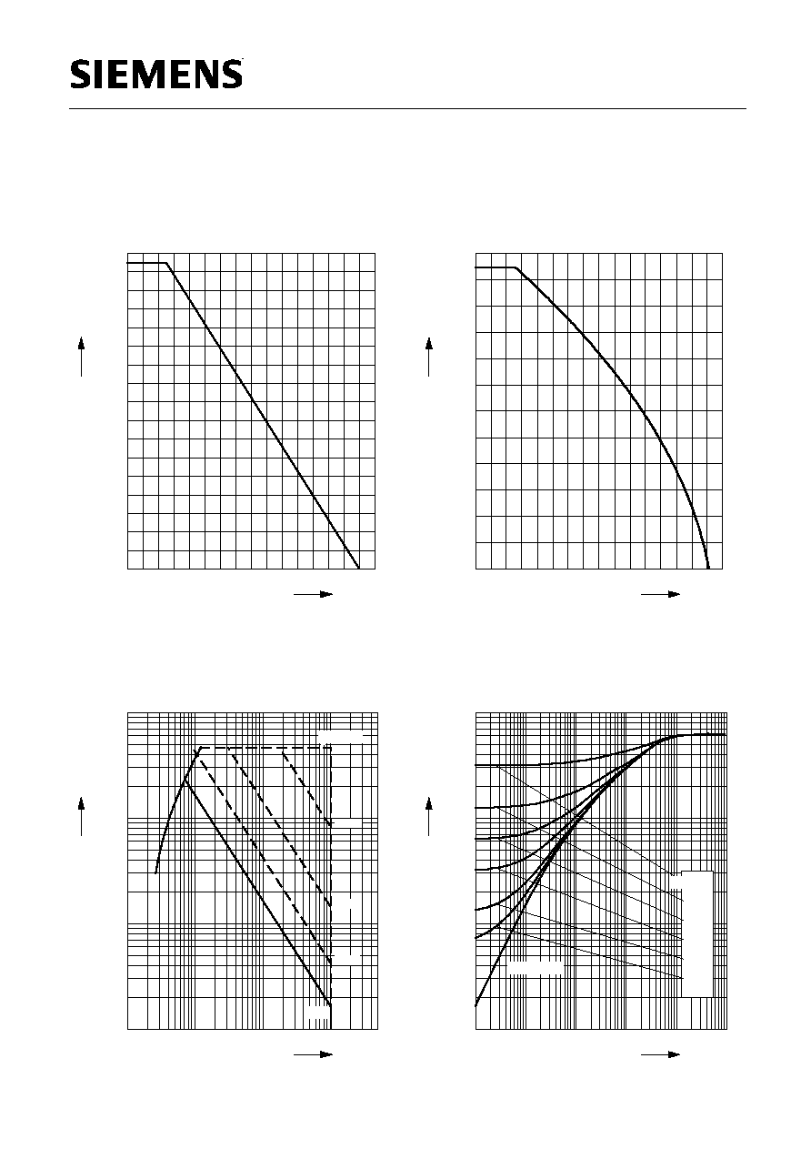
Power dissipation
P
tot
=
(
T
C
)
parameter:
T
j
150 ∞C
0
20
40
60
80
100
120
∞C
160
T
C
0
20
40
60
80
100
120
140
W
170
P
tot
Collector current
I
C
=
(
T
C
)
parameter:
V
GE
15 V ,
T
j
150 ∞C
0
20
40
60
80
100
120
∞C
160
T
C
0
2
4
6
8
10
12
14
16
18
20
A
24
I
C
Safe operating area
I
C
=
(
V
CE
)
parameter:
D = 0, T
C
= 25∞C ,
T
j
150 ∞C
-1
10
0
10
1
10
2
10
A
I
C
10
0
10
1
10
2
10
3
V
V
CE
DC
10 ms
1 ms
100 µs
t
p
= 16.0µs
Transient thermal impedance IGBT
Z
th JC
=
(
t
p
)
parameter:
D = t
p
/
T
-3
10
-2
10
-1
10
0
10
K/W
Z
thJC
10
-5
10
-4
10
-3
10
-2
10
-1
10
0
s
t
p
single pulse
0.01
0.02
0.05
0.10
0.20
D = 0.50
Semiconductor Group
5
Dec-06-1995
BUP 203
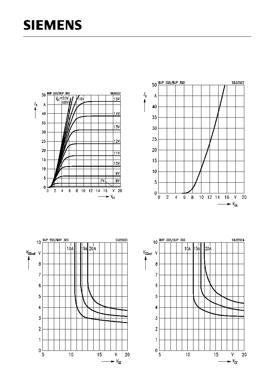
Typ. output characteristics
I
C
= f
(
V
CE
)
parameter:
t
p
= 80 µs,
T
j
= 125 ∞
C
Typ. transfer characteristics
I
C
= f (V
GE
)
parameter:
t
P
= 80 µs,
V
CE
= 20 V,
T
j
= 25 ∞C
Typ. saturation characteristics
V
CE(sat)
=
f (V
GE
)
parameter:
T
j
= 25 ∞C
Typ. saturation characteristics
V
CE(sat)
=
f (
V
GE
)
parameter:
T
j
= 125 ∞C
Semiconductor Group
6
Dec-06-1995
BUP 203
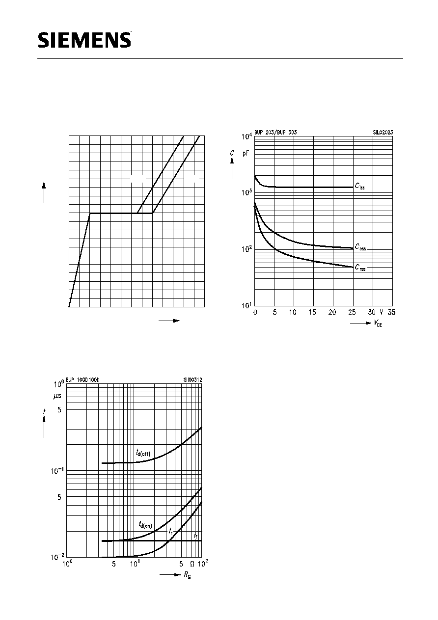
Typ. gate charge
V
GE
=
(
Q
Gate
)
parameter:
I
C puls
= 10 A
0
20
40
60
80
100
nC
130
Q
Gate
0
2
4
6
8
10
12
14
16
V
20
V
GE
800 V
400 V
Typ. capacitances
C = f (V
CE
)
parameter:
V
GE
= 0 V,
f = 1 MHz
Typ. switching time
t = f (R
G
), inductive load, T
j
= 125 ∞C
parameter:
V
CE
= 600 V,
V
GE
= ± 15 V,
I
C
= 10 A
Semiconductor Group
7
Dec-06-1995
BUP 203
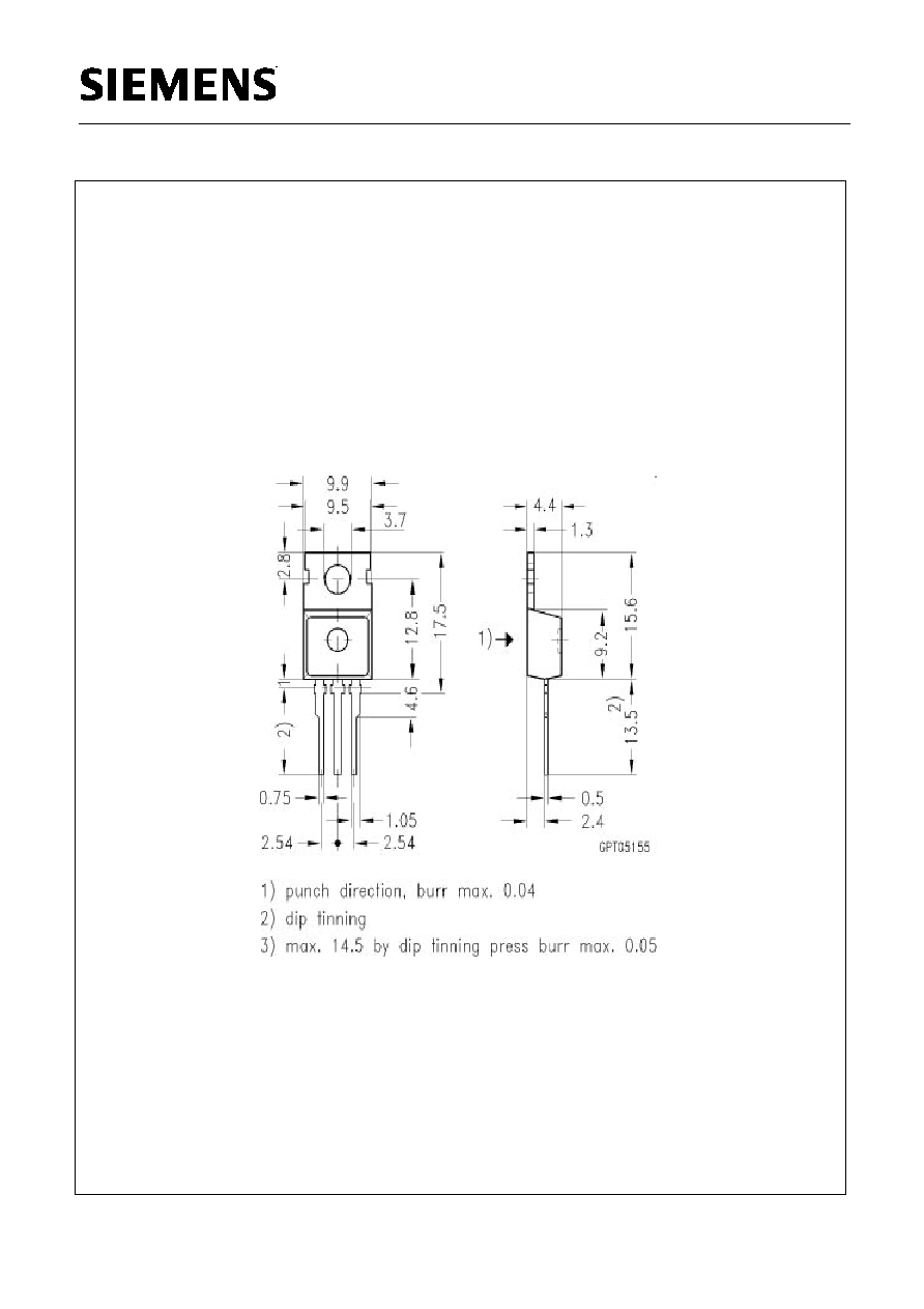
Package Outlines
Dimensions in mm
Weight: 8 g