175 GREAT VALLEY PKWY. MALVERN, PA 19355
U S A
SPT402 125mm
SPT402 125mm
SPT402 125mm
SPT402 125mm
SPT402 125mm THYRIST
THYRIST
THYRIST
THYRIST
THYRISTO R
O R
O R
O R
O R
5000V 4600A
5000V 4600A
5000V 4600A
5000V 4600A
5000V 4600A
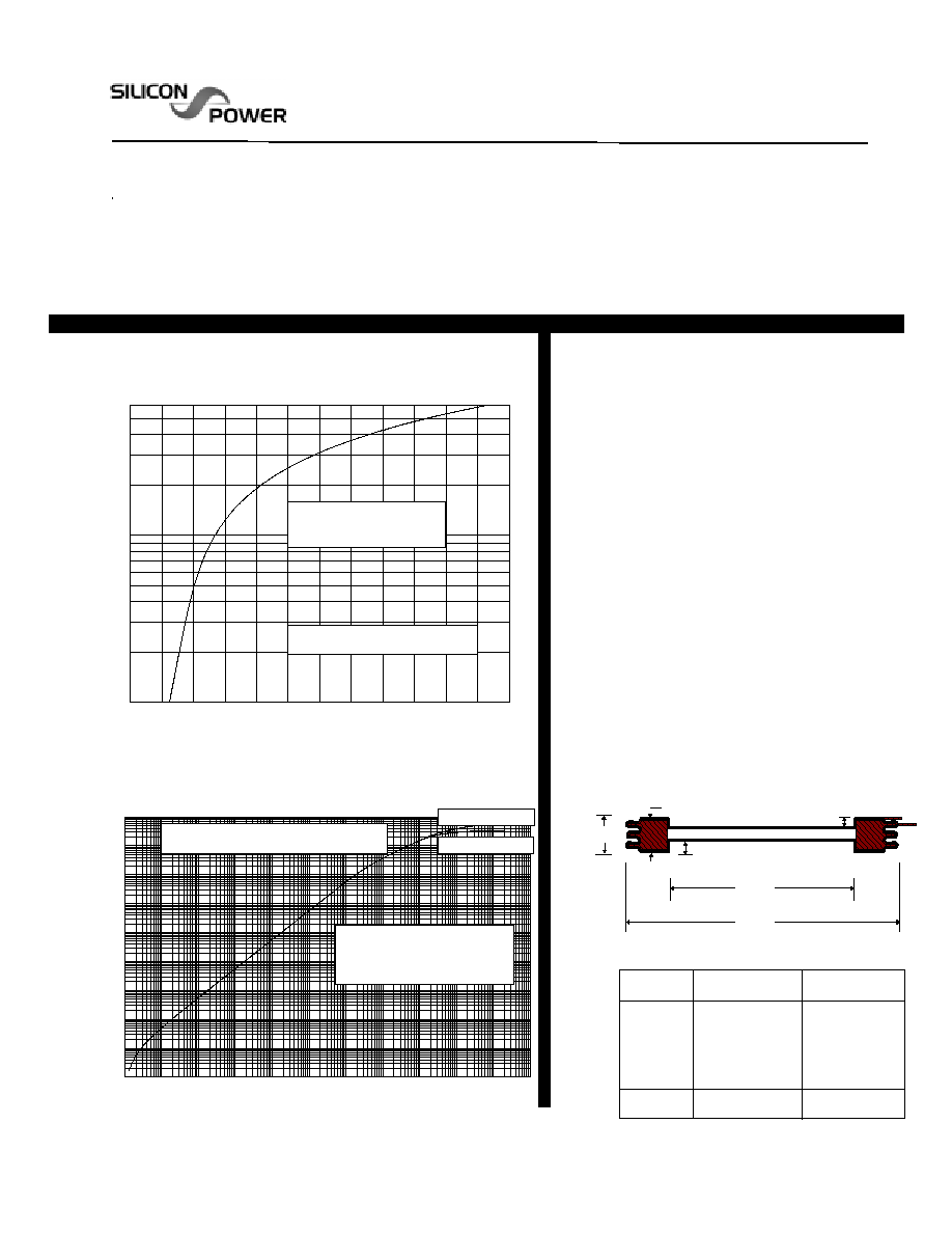
ON-STATE CHARACTERISTIC
Process Maximum
1000
10000
0
1
2
3
4
5
6
7
8
9
10
11
12
On-State Current, It (A)
On-State Voltage, Vt (volts)
On-State Voltage, Vt (volts)
96h:t402onst
Process Maximum
Tcase = 115 C
8.3 ms pulses
60000
special - involute gate
96h:pm4
Maximum Off-State & Reverse
Blocking Voltage Ratings
T
J
= 0 to 115
o
C
V
DRM
V
RRM
(volts)
SPT402_HT
5000
5000
SPT402_HS
4900
4900
SPT402_HR
4800
4800
SPT402_HP
4700
4700
SPT402_HM
4600
4600
SPT402_HK
4500
4500
rev 4 2/10/2000
1.000E-11
1.000E-10
1.000E-09
1.000E-08
1.000E-07
1.000E-06
1.000E-05
1.000E-04
1.000E-03
0.01
THERMAL IMPEDANCE vs. ON-TIME
Zthj-c (deg C/W)
On-Time (seconds)
On-Time (seconds)
96h:12/11/96
1E-8
1E-7
1E-6 1E-5 1E-4
.001
.01
.1
1.
10
to sink*
to case
Model SPT402 with Involute gate
.0051
.0034
* double sided cooling
through external copper
post inserts
The SPT402 thyristor features a multi-arm involute gate which can be triggered with 5 - 10 A gate pulses by means of an integrated
pilot gate or directly fired using 50 - 100A gate pulses. The involute pattern affords full area conduction in minimum time while
a corresponding high di/dt rating depends on the choice of gating method. The factory setting for either pilot triggered or gate
triggered version, internal to the package, is an option when ordering by keying it to the model number code. The design utilizes
a new termination technique, SPCO's revolutioary Light Silicon Sandwich, LSS technology, which eliminates heavy refractory
metal as a substrate while retaining the alloyed anode interface necessary for high surge current duty. This thyristor is supplied
in a reliable plastic light weight package allowing the insertion of liquid cooled chillers. Solid copper inserts can be ordered
for adjoining air cooled heat dissipators using commercially available clamping hardware.
Optional external posts drw. # 0215B8315
Ni plated copper, 0.35" thick each
Compressed thickness including external posts
0.87" - 0.88"
External clamping force
25000 lb minimum
Internal gate connection:
Pilot
SPT402A (see page 2 for gate drive)
Direct
SPT402B
"
"
Weight: 18oz without posts
3 lb 10 oz with posts
C
D
D
B
A
Nominal Dimensions
A
B
C
D
inch
mm
6
162.7
106.4
20.24
7.77
13/32
3/16
51/64
4
dia.
dia.
dia.
dia.
C
0.3061
LIMITING CHARACTERISTICS AND RATINGS
LIMITING CHARACTERISTICS AND RATINGS
LIMITING CHARACTERISTICS AND RATINGS
LIMITING CHARACTERISTICS AND RATINGS
LIMITING CHARACTERISTICS AND RATINGS
96h: sh 2, Rev 4; 2/10/2000
SPT402
SPT402
SPT402
SPT402
SPT402
10
100
1000
1
10
100
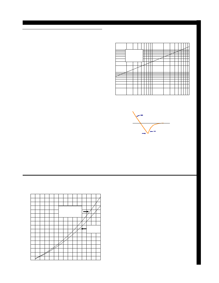
Peak Recovery Current Relationship
with Commutating di/dt
Peak Recovery Current, Irm, (A)
Commutating di/dt, (A/us)
Commutating di/dt, (A/us)
2000
Process Limit
Itm = 100 kA
Tj = 115 C
di
dt
di
dt
RM
(REC)
t
Snappiness
F = di/dt(rec) / di/dt
I
3000
1547
1727
4000
2233
2493
5000
2978
3331
6000
3783
4246
7000
4650
5241
8000
5580
6319
9000
6577
7483
10000
7641
8735
11000
8775
10078
12000
9981
11516
13000
11259
13048
14000
12612
14679
15000
14042
16408
1000
369
424
2000
921
1035
I
T
(peak)
half-sine
3ph
180
o
120
o
amperes
watts
watts
FULL CYCLE AVERAGE POWER LOSS
50 / 60 Hz T
J
= 115
o
C
0
1
2
3
4
5
6
7
8
9
10
11
12
13
14
15
16
17
0
1
2
3
4
5
6
7
8
9
10 11 12 13 14 15
FULL CYCLE AVERAGE POWER LOSS
versus
PEAK CURRENT at 50/60 Hz
Pavg (kilowatts)
Peak Current, It (kA)
Peak Current, It (kA)
96h
(plasma spreading and conduction loss)
overlap angle
= 20 degree
180 degree
sinewave
120 deg.sq. wave
Tj = 115 degC
Gate Pulse: 15us duration / 0.5us rise time
SPT402A
SPT402B
di/dt
<=100A/us
<1000A/us
1000-4000A/us
V
OC
50 V
100 V
100 V
I
SS
5 A
200 A
400 A
Repetitive peak off-
Repetitive peak off-
Repetitive peak off-
Repetitive peak off-
Repetitive peak off-
V
V
V
V
V
D R M
D R M
D R M
D R M
D R M
T
T
T
T
T
J
J
J
J
J
=0
=0
=0
=0
=0
up to
up to
up to
up to
up to
V
V
V
V
V
state & reverse volts
state & reverse volts
state & reverse volts
state & reverse volts
state & reverse volts
V
V
V
V
V
R R M
R R M
R R M
R R M
R R M
to 115
to 115
to 115
to 115
to 115
o
o
o
o
o
C
C
C
C
C
5000
5000
5000
5000
5000
Repetitive working
Repetitive working
Repetitive working
Repetitive working
Repetitive working
V
V
V
V
V
D W M
D W M
D W M
D W M
D W M
T
T
T
T
T
J
J
J
J
J
=0
=0
=0
=0
=0
0.8V
0.8V
0.8V
0.8V
0.8V
D R M
D R M
D R M
D R M
D R M
V
V
V
V
V
crest voltage
crest voltage
crest voltage
crest voltage
crest voltage
V
V
V
V
V
R W M
R W M
R W M
R W M
R W M
to 115
to 115
to 115
to 115
to 115
o
o
o
o
o
C
C
C
C
C
0.8V
0.8V
0.8V
0.8V
0.8V
R R M
R R M
R R M
R R M
R R M
Repetitive peak off-
Repetitive peak off-
Repetitive peak off-
Repetitive peak off-
Repetitive peak off-
I
I
I
I
I
D W M
D W M
D W M
D W M
D W M
T
T
T
T
T
J
J
J
J
J
=0
=0
=0
=0
=0
250
250
250
250
250
m a
m a
m a
m a
m a
state & reverse current
state & reverse current
state & reverse current
state & reverse current
state & reverse current I
I
I
I
I
R W M
R W M
R W M
R W M
R W M
to 115
to 115
to 115
to 115
to 115
o
o
o
o
o
C
C
C
C
C
100
100
100
100
100
Average on-state
Average on-state
Average on-state
Average on-state
Average on-state
I
I
I
I
I
T(AV)
T(AV)
T(AV)
T(AV)
T(AV)
T
T
T
T
T
case
case
case
case
case
=
=
=
=
=
4600
4600
4600
4600
4600
A
A
A
A
A
current
current
current
current
current
70
70
70
70
70
o
o
o
o
o
C
C
C
C
C
Peak half-cycle
Peak half-cycle
Peak half-cycle
Peak half-cycle
Peak half-cycle
I
I
I
I
I
T S M
T S M
T S M
T S M
T S M
8.3 ms
8.3 ms
8.3 ms
8.3 ms
8.3 ms
60
60
60
60
60
kA
kA
kA
kA
kA
non-rep surge current
non-rep surge current
non-rep surge current
non-rep surge current
non-rep surge current
1.5 ms
1.5 ms
1.5 ms
1.5 ms
1.5 ms
100
100
100
100
100
T
T
T
T
T
J
J
J
J
J
=115
=115
=115
=115
=115
o
o
o
o
o
C
C
C
C
C
On-state voltage
On-state voltage
On-state voltage
On-state voltage
On-state voltage
V
V
V
V
V
T M
T M
T M
T M
T M
I
I
I
I
I
T
T
T
T
T
=4000A
=4000A
=4000A
=4000A
=4000A
1.90
1.90
1.90
1.90
1.90
V
V
V
V
V
t
t
t
t
t
P
P
P
P
P
=8.3ms
=8.3ms
=8.3ms
=8.3ms
=8.3ms
T
T
T
T
T
J
J
J
J
J
=115
=115
=115
=115
=115
o
o
o
o
o
C
C
C
C
C
Critical gate trigger
Critical gate trigger
Critical gate trigger
Critical gate trigger
Critical gate trigger
I
I
I
I
I
G T
G T
G T
G T
G T
V
V
V
V
V
D
D
D
D
D
= 12 V
= 12 V
= 12 V
= 12 V
= 12 V
150
150
150
150
150
m a
m a
m a
m a
m a
current / voltage
current / voltage
current / voltage
current / voltage
current / voltage
V
V
V
V
V
G T
G T
G T
G T
G T
T
T
T
T
T
J
J
J
J
J
= 25
= 25
= 25
= 25
= 25
o
o
o
o
o
C
C
C
C
C
5.0
5.0
5.0
5.0
5.0
V
V
V
V
V
Non-trigger gate
Non-trigger gate
Non-trigger gate
Non-trigger gate
Non-trigger gate
I
I
I
I
I
G D
G D
G D
G D
G D
V
V
V
V
V
D
D
D
D
D
= 2000V
= 2000V
= 2000V
= 2000V
= 2000V
15
15
15
15
15
m a
m a
m a
m a
m a
current
current
current
current
current
V
V
V
V
V
G D
G D
G D
G D
G D
T
T
T
T
T
J
J
J
J
J
= 115
= 115
= 115
= 115
= 115
o
o
o
o
o
C
C
C
C
C
0.8
0.8
0.8
0.8
0.8
V
V
V
V
V
Maximum peak
Maximum peak
Maximum peak
Maximum peak
Maximum peak
I
I
I
I
I
R M
R M
R M
R M
R M
di/dt = 2 A/us
di/dt = 2 A/us
di/dt = 2 A/us
di/dt = 2 A/us
di/dt = 2 A/us
110
110
110
110
110
A
A
A
A
A
recovery current
recovery current
recovery current
recovery current
recovery current
T
T
T
T
T
J
J
J
J
J
= 115
= 115
= 115
= 115
= 115
o
o
o
o
o
C
C
C
C
C
snappiness F = 2-3
snappiness F = 2-3
snappiness F = 2-3
snappiness F = 2-3
snappiness F = 2-3
Critical rate of rise
Critical rate of rise
Critical rate of rise
Critical rate of rise
Critical rate of rise
di/dt
di/dt
di/dt
di/dt
di/dt
T
T
T
T
T
J
J
J
J
J
=115
=115
=115
=115
=115
o
o
o
o
o
C SPT402A
C SPT402A
C SPT402A
C SPT402A
C SPT402A 100
100
100
100
100
A/us
A/us
A/us
A/us
A/us
of on-state current
of on-state current
of on-state current
of on-state current
of on-state current
rep
rep
rep
rep
rep
60 Hz SPT402B 4000
60 Hz SPT402B 4000
60 Hz SPT402B 4000
60 Hz SPT402B 4000
60 Hz SPT402B 4000
incl. 60A snubber discharge
incl. 60A snubber discharge
incl. 60A snubber discharge
incl. 60A snubber discharge
incl. 60A snubber discharge
Critical rate of rise
Critical rate of rise
Critical rate of rise
Critical rate of rise
Critical rate of rise
dv/dt
dv/dt
dv/dt
dv/dt
dv/dt
T
T
T
T
T
J
J
J
J
J
=115
=115
=115
=115
=115
o
o
o
o
o
C
C
C
C
C
1000
1000
1000
1000
1000
V/us
V/us
V/us
V/us
V/us
of off-state voltage
of off-state voltage
of off-state voltage
of off-state voltage
of off-state voltage
V
V
V
V
V
D
D
D
D
D
= 67% V
= 67% V
= 67% V
= 67% V
= 67% V
D R M
D R M
D R M
D R M
D R M
Turn-on delay
Turn-on delay
Turn-on delay
Turn-on delay
Turn-on delay
t
t
t
t
t
d
d
d
d
d
V
V
V
V
V
D
D
D
D
D
= 50%V
= 50%V
= 50%V
= 50%V
= 50%V
D R M
D R M
D R M
D R M
D R M
4
4
4
4
4
us
us
us
us
us
T
T
T
T
T
J
J
J
J
J
=115
=115
=115
=115
=115
o
o
o
o
o
C
C
C
C
C
Turn-off time
Turn-off time
Turn-off time
Turn-off time
Turn-off time
T
T
T
T
T
off
off
off
off
off
5A/us,-100V
5A/us,-100V
5A/us,-100V
5A/us,-100V
5A/us,-100V
400
400
400
400
400
us
us
us
us
us
20V/us to 2000V
20V/us to 2000V
20V/us to 2000V
20V/us to 2000V
20V/us to 2000V