
ST
Sitronix
ST7070
Dot Matrix LCD Controller/Driver
V0.8
2003/11/10
1/50
Features
5 x 8 dot matrix possible
Low power operation support:
-- 2.7 to 5.5V
Wide range of LCD driver power
-- 3.0 to 7.0V
Support high speed serial interface
Correspond to high speed MPU bus
interface
-- 2 MHz (when V
CC
= 5V)
80 x 9-bit display RAM (80 characters max.)
19840-bit character generator ROM for a
total of 496 character fonts(5 x 8 dot)
64 x 8-bit character generator RAM
-- 8 character fonts (5 x 8 dot)
16-common x 80-segment liquid crystal
display driver
Programmable duty cycles
-- 1/8 for one line of 5 x 8 dots with cursor
-- 1/16 for two lines of 5 x 8 dots & cursor
Wide range of instruction functions:
Display clear, cursor home, display on/off,
cursor on/off, cursor shift, display shift
Automatic reset circuit that initializes the
controller/driver after power on
Internal oscillator with external resistors
Low power consumption
Description
The ST7070 dot-matrix liquid crystal display
controller and driver LSI displays alphanumeric,
Japanese kana characters, and symbols. It can be
configured to drive a dot-matrix liquid crystal display
under the control of a 4- or 8-bit microprocessor. With
high speed serial interface(3-line SPI , 4-line SPI), the
external MCU can control ST7070 directly. Since all
the functions such as display RAM, character
generator, and liquid crystal driver, required for
driving a dot-matrix liquid crystal display are internally
provided on one chip, a minimal system can be
interfaced with this controller/driver.
The ST7070 has function partial compatibility with the
HD44780, KS0066 and SED1278 that allows the user
to easily replace it with an ST7070. The ST7070
character generator ROM is extended to generate
496 5x8 dot character fonts for a total of 496 different
character fonts. The low power supply (2.7V to 5.5V)
of the ST7070 is suitable for any portable
battery-driven product requiring low power
dissipation.
The ST7070 LCD driver consists of 16 common
signal drivers and 80 segment signal drivers which
can extend display size by cascading segment driver
ST7921. The maximum display size can be either 80
characters in 1-line display or 40 characters in 2-line
display. A single ST7070 can display up to one
16-character line or two 16-character lines.

ST7070
V0.8
2003/11/10
2/51
ST7070 Serial Specification Revision History
Version Date
Description
0.1-
Preliminary
2002/9/23 Preliminary
version
0.1-
Preliminary
2002/11/21 Add 3-line SPI interface
0.2-
Preliminary
2002/12/20
1.
N substrate change to P substrate.
2.
Pad location modify.
0.3-
Preliminary
2003/01/21
Modify "Supply Voltage for LCD Drive" Description
I/O Pad Configuration
0.4-
Preliminary
2003/2/18 Add Application circuit
0.5
2003/07/24 Modify the 4 bit interface Initializing flow by Instruction
0.6
2003/08/28 Change the font Table (0B)
0.7
2003/09/09 Add the DC Characteristics Note
0.8 2003/11/10
Modify the 4 bit interface Initializing flow by Instruction
Add serial interface Initializing flow
ST7070
V0.8
2003/11/10
3/51
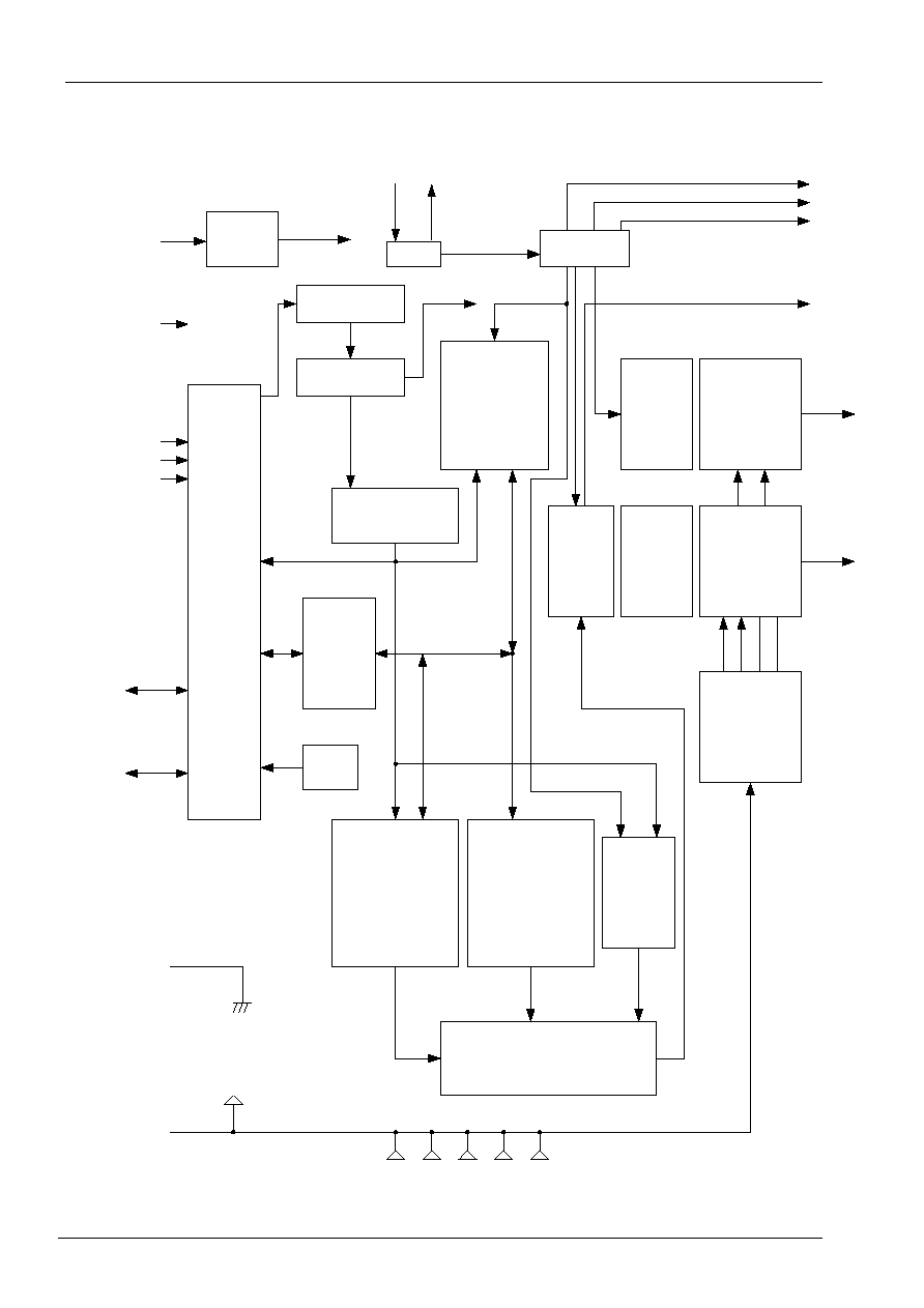
Block Diagram
Reset
circuit
CPG
Timing
generator
Instruction
register(IR)
Instruction
decoder
Display data
RAM
(DDRAM)
80x9 bits
16-bit
shift
register
Common
signal
driver
80-bit
latch
circuit
80-bit
shift
register
Segment
signal
driver
LCD drive
voltage
selector
Address
counter
Data
register
(DR)
Busy
flag
MPU
interface
Input/
output
buffer
Character
generator
RAM
(CGRAM)
64 bytes
Character
generator
ROM
(CGROM)
19840 bits
Cursor
and
blink
controller
Parallel/serial converter
and
attribute circuit
RS
RW
E
DB4 to
DB7
DB0 to
DB3
GND
Vcc
V0
V1
V2
V3
V4
OSC1 OSC2
CL1
CL2
M
D
COM1 to
COM16
SEG1 to
SEG80
XRESET
PSB

ST7070
V0.8
2003/11/10
4/51
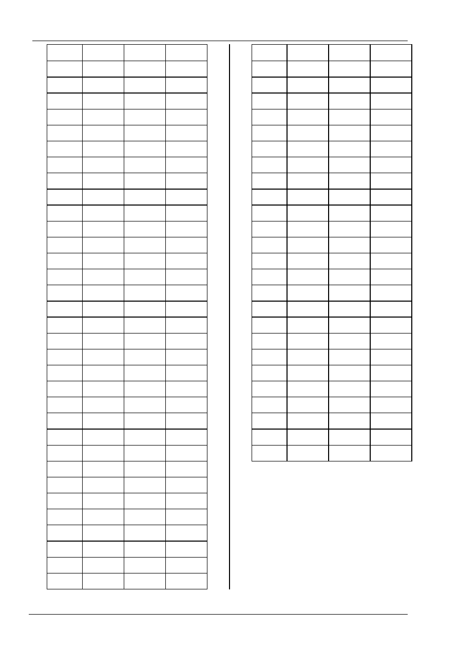
Pad Arrangement
Substrate must connect to "Vss".
Mark

ST7070
V0.8
2003/11/10
5/51
Pad Configuration
Pad No.
Function
X
Y
001 RS
-2585
660
002 DB[7]
-2585
540
003 XRESET -2585
430
004 DB[6]
-2585
320
005 DB[5]
-2585
210
006 DB[4]
-2585
105
007 DB[3]
-2585
0
008 DB[2]
-2585
-105
009 DB[1]
-2585
-210
010 DB[0]
-2585
-320
011 PSB
-2585
-430
012 RW
-2585
-540
013 E
-2585
-660
014 COM[9] -2585
-790
015 COM[10] -2445
-790
016 COM[11] -2315
-790
017 COM[12] -2195
-790
018 COM[13] -2085
-790
019 COM[14] -1975
-790
020 COM[15] -1865
-790
021 COM[16] -1755
-790
022 SEG[41] -1645
-790
023 SEG[42] -1535
-790
024 SEG[43] -1425
-790
025 SEG[44] -1315
-790
026 SEG[45] -1208
-790
027 SEG[46] -1102
-790
028 SEG[47] -997
-790
029 SEG[48] -892
-790
030 SEG[49] -787
-790
031 SEG[50] -682
-790
032 SEG[51] -577
-790
Pad No.
Function
X
Y
033 SEG[52] -472
-790
034 SEG[53] -367
-790
035 SEG[54] -262
-790
036 SEG[55] -157
-790
037 SEG[56] -52
-790
038 SEG[57] 52
-790
039 SEG[58] 157
-790
040 SEG[59] 262
-790
041 SEG[60] 367
-790
042 SEG[61] 472
-790
043 SEG[62] 577
-790
044 SEG[63] 682
-790
045 SEG[64] 787
-790
046 SEG[65] 892
-790
047 SEG[66] 997
-790
048 SEG[67] 1102
-790
049 SEG[68] 1207
-790
050 SEG[69] 1315
-790
051 SEG[70] 1425
-790
052 SEG[71] 1535
-790
053 SEG[72] 1645
-790
054 SEG[73] 1755
-790
055 SEG[74] 1865
-790
056 SEG[75] 1975
-790
057 SEG[76] 2085
-790
058 SEG[77] 2195
-790
059 SEG[78] 2315
-790
060 SEG[79] 2445
-790
061 SEG[80] 2585
-790
062 D
2585
-660
063 M
2585
-540
064 CL2
2585
-430
ST7070
V0.8
2003/11/10
6/51
Pad No.
Function
X
Y
065 CL1
2585
-320
066 OSC2 2585
-210
067 OSC1 2585
-105
068 VSS
2585
0
069 V4
2585
105
070 V3
2585
210
071 V2
2585
320
072 V1
2585
430
073 V0
2585
540
074 VDD
2585
660
075 SEG[40] 2585
790
076 SEG[39] 2445
790
077 SEG[38] 2315
790
078 SEG[37] 2195
790
079 SEG[36] 2085
790
080 SEG[35] 1975
790
081 SEG[34] 1865
790
082 SEG[33] 1755
790
083 SEG[32] 1645
790
084 SEG[31] 1535
790
085 SEG[30] 1425
790
086 SEG[29] 1315
790
087 SEG[28] 1207
790
088 SEG[27] 1102
790
089 SEG[26] 997
790
090 SEG[25] 892
790
091 SEG[24] 787
790
092 SEG[23] 682
790
093 SEG[22] 577
790
094 SEG[21] 472
790
095 SEG[20] 367
790
096 SEG[19] 262
790
097 SEG[18] 157
790
Pad No.
Function
X
Y
098 SEG[17] 52
790
099 SEG[16] -52
790
100 SEG[15] -157
790
101 SEG[14] -262
790
102 SEG[13] -367
790
103 SEG[12] -472
790
104 SEG[11] -577
790
105 SEG[10] -682
790
106 SEG[9] -787
790
107 SEG[8] -892
790
108 SEG[7] -997
790
109 SEG[6] -1102
790
110 SEG[5] -1208
790
111 SEG[4] -1315
790
112 SEG[3] -1425
790
113 SEG[2] -1535
790
114 SEG[1] -1645
790
115 COM[1] -1755
790
116 COM[2] -1865
790
117 COM[3] -1975
790
118 COM[4] -2085
790
119 COM[5] -2195
790
120 COM[6] -2315
790
121 COM[7] -2445
790
122 COM[8] -2585
790
ST7070
V0.8
2003/11/10
7/51
Pin Function
Name Number
I/O
Interfaced
with
Function
RS 1
I
MPU
Select registers.
0: Instruction register (for write) Busy flag:
address counter (for read)
1: Data register (for write and read)
When serial interface select ,RS pull low , not floating.
R/W 1
I
MPU
Select read or write.
0: Write 1: Read
When serial interface select ,R/W pull low, not floating.
E 1
I
MPU
Starts data read/write.
When serial interface select ,E pull height , not floating.
XRESET
1
I
MPU
Hardware reset pin, Low active
PSB
1
I
MPU
Parallel /Serial selection. PSB: "1" Parallel , "0" Serial.
DB4 to DB7
4
I/O
MPU
Four high order bi-directional tristate data bus pins. Used for
data transfer and receive between the MPU and the ST7070.
DB7 can be used as a busy flag.
Serial:
DB7:data input pin for serial mode(SI)
DB6:serial clock input for serial mode(SCL)
DB5:chip select pin for serial mode(/CS)
When serial interface select ,D4 pull height , not floating.
4bits mode : These pins are used during 4-bit operation.
DB0 to DB3
4
I/O
MPU
Four low order bi-directional tristate data bus
pins. Used for data transfer and receive
between the MPU and the ST7070.
These pins are not used during 4-bit operation and serial
interface , must pull height , not floating.
CL1 1
O
Extension
driver
Clock to latch serial data D sent to the
Extension driver
CL2
1
O
Extension driver Clock to shift serial data D
M
1 O
Extension
driver
Switch signal for converting the liquid crystal
drive waveform to AC
D 1
O
Extension
driver
Character pattern data corresponding to each
segment signal
COM1 to
COM16
16
O
LCD
Common signals that are not used are changed
to non-selection waveform. COM9 to COM16
are non-selection waveforms at 1/8 duty factor
and COM12 to COM16 are non-selection
waveforms at 1/11 duty factor.
SEG1 to
SEG80
80 O LCD
Segment signals
V0 to V4
5
-
Power supply
Power supply for LCD drive
V0
Vss = 10 V (Max)
V
CC
, GND
2
-
Power supply
V
CC
: 2.7V to 5.5V, GND: 0V
OSC1, OSC2
2
Oscillation
resistor clock
When crystal oscillation is performed, a resistor
must be connected externally. When the pin
input is an external clock, it must be input to OSC1.
Note:
1. V0 >= V1 >= V2 >= V3 >= V4 >= Vss must be maintained
2. Two clock options:
R
OSC1
OSC2
OSC2
Clock
input
R=91K
(Vcc=5V)
R=75K
(Vcc=3V)
OSC1

ST7070
V0.8
2003/11/10
8/51
Function Description
System Interface
This chip has all two kinds of interface type with MPU : 4-bit bus and 8-bit bus. 4-bit bus or 8-bit bus is selected by DL
bit in the instruction register.
During read or write operation, two 8-bit registers are used. One is data register (DR), the other is instruction
register(IR).
The data register(DR) is used as temporary data storage place for being written into or read from DDRAM/CGRAM,
target RAM is selected by RAM address setting instruction. Each internal operation, reading from or writing into RAM,
is done automatically. So to speak, after MPU reads DR data, the data in the next DDRAM/CGRAM address is
transferred into DR automatically. Also after MPU writes data to DR, the data in DR is transferred into
DDRAM/CGRAM automatically.
The Instruction register(IR) is used only to store instruction code transferred from MPU. MPU cannot use it to read
instruction data.
To select register, use RS input pin in 4-bit/8-bit bus mode.
Table 1. Various kinds of operations according to RS and R/W bits.
Busy Flag (BF)
When BF = "High", it indicates that the internal operation is being processed. So during this time the next instruction
cannot be accepted. BF can be read, when RS = Low and R/W = High (Read Instruction Operation), through DB7 port.
Before executing the next instruction, be sure that BF is not High.
Address Counter (AC)
Address Counter(AC) stores DDRAM/CGRAM address, transferred from IR.
After writing into (reading from) DDRAM/CGRAM, AC is automatically increased (decreased) by 1.
When RS = "Low" and R/W = "High", AC can be read through DB6 ~ DB0 ports.
RS R/W
Operation
L L
Instruction Write operation (MPU writes Instruction code
into IR)
L
H Read Busy Flag(DB7) and address counter (DB6 ~ DB0)
H
L Data Write operation (MPU writes data into DR)
H
H Data Read operation (MPU reads data from DR)

ST7070
V0.8
2003/11/10
9/51
Display Data RAM (DDRAM)
Display data RAM (DDRAM) stores display data represented in 9-bit character codes. Its extended capacity is 80 x 9
bits, or 80 characters. The area in display data RAM (DDRAM) that is not used for display can be used as general data
RAM. See Figure 1 for the relationships between DDRAM addresses and positions on the liquid crystal display.
The DDRAM address (A
DD
) is set in the address counter (AC) as hexadecimal.
1-line display (N = 0) (Figure 2)
When there are fewer than 80 display characters, the display begins at the head position. For
example, if using only the ST7070, 8 characters are displayed. See Figure 3.
When the display shift operation is performed, the DDRAM address shifts. See Figure 3.
Figure 1 DDRAM Address
Figure 2 1-Line Display
Figure 3 1-Line by 8-Character Display Example
AC6
AC5 AC4
AC3
AC2
AC1 AC0
1
0
0
1
1
1
1
High Order
bits
Low Order
bits
AC
Example: DDRAM Address 4F
00
01
02
03
04
05
4D 4E 4F
DDRAM Address
....................
1
2
3
4
5
6
80
79
78
Display
Position
(Digit)
00
01
02
03
04
05
06
07
DDRAM
Address
1
2
3
4
5
6
8
7
Display
Position
08
01
02
03
04
05
06
07
00
01
02
03
04
05
06
4F
For
Shift Left
For
Shift Right

ST7070
V0.8
2003/11/10
10/51
2-line display (N = 1) (Figure 4)
Figure 4 2-Line Display
Case 1: When the number of display characters is less than 40
�
2 lines, the two lines are
displayed from the head. Note that the
first line end address and th
e second line start address are not consecutive. For
example, when just the ST7070 is used, 16
characters
�
2 lines are displayed.
See Figure 5.
When display shift operation is performed, the DDRAM address shifts. See Figure 5.
Figure 5 2-Line by 16-Character Display Example
Case 2: For a 16-character
� 2-line display, See Figure 5.
When display shift operation is performed, the DDRAM address shifts. See Figure 5.
DDRAM
Address
(hexadecimal)
00
01
02
03
04
05
25
26
27
....................
1
2
3
4
5
6
40
39
38
Display
Position
40
41
42
43
44
45
65
66
67
....................
DDRAM
Address
Display
Position
For
Shift
Right
00
01
02
03
04
05
06
07
1
2
3
4
5
6
8
7
40
41
42
43
44
45
46
47
For
Shift
Left
08
01
02
03
04
05
06
07
48
41
42
43
44
45
46
47
00
01
02
03
04
05
06
27
40
41
42
43
44
45
46
67
08
09 0A 0B 0C 0D 0E
0F
9
10
11
12
13
14
16
15
48
49 4A 4B 4C 4D 4E
4F
10
09 0A 0B 0C 0D 0E 0F
50
49 4A 4B 4C 4D 4E 4F
08
09 0A 0B 0C 0D
0E
07
48
49 4A 4B 4C 4D
4E
47

ST7070
V0.8
2003/11/10
11/51
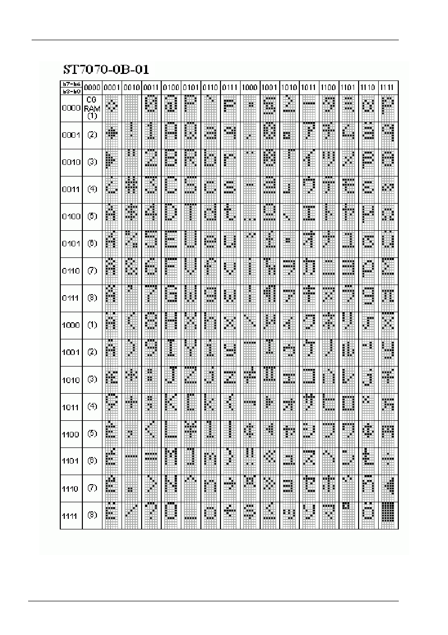
Character Generator ROM (CGROM)
The character generator ROM generates 5 x 8 dot character patterns from 9-bit character codes. It can generate 496
5 x 8 dot character patterns. User-defined character patterns are also available by mask-programmed ROM.
Character Generator RAM (CGRAM)
In the character generator RAM, the user can rewrite character patterns by program. For 5 x 8 dots, eight character
patterns can be written.
Write into DDRAM the character codes at the addresses shown as the left column of Table 4 to show the character
patterns stored in CGRAM.
See Table 5 for the relationship between CGRAM addresses and data and display patterns. Areas that are not used
for display can be used as general data RAM.
Timing Generation Circuit
The timing generation circuit generates timing signals for the operation of internal circuits such as
DDRAM, CGROM and CGRAM. RAM read timing for display and internal operation timing by MPU
access are generated separately to avoid interfering with each other. Therefore, when writing data to
DDRAM, for example, there will be no undesirable interference, such as flickering, in areas other than
the display area.
LCD Driver Circuit
LCD Driver circuit has 16 common and 80 segment signals for LCD driving. Data from CGRAM/CGROM is
transferred to 80 bit segment latch serially, and then it is stored to 80 bit shift latch. When each common is selected by
16 bit common register, segment data also output through segment driver from 80 bit segment latch. In case of 1-line
display mode, COM1 ~ COM8 have 1/8 duty, and in 2-line mode, COM1 ~ COM16 have 1/16 duty ratio.
Cursor Control Circuit
It can generate the cursor in the cursor control circuit. The cursor or the blink appears in the digit at the display data
RAM address set in the address counter.
ST7070
V0.8
2003/11/10
12/51
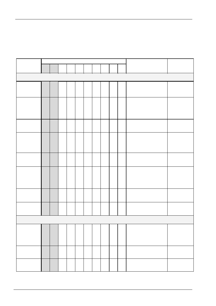
Table 4 Correspondence between Character Codes and Character Patterns (Page 1)
(b8=0)

ST7070
V0.8
2003/11/10
13/51
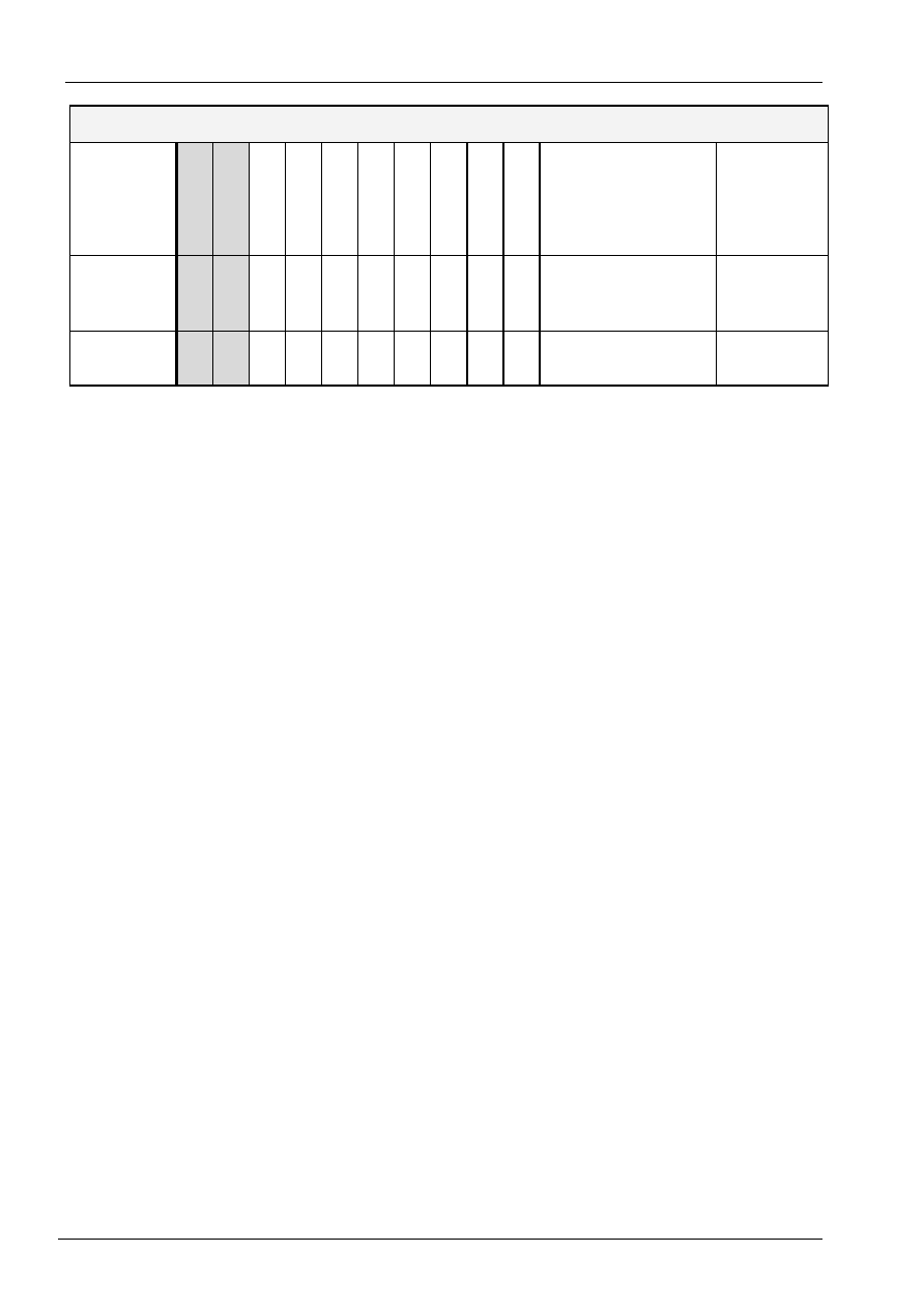
Table 4 Correspondence between Character Codes and Character Patterns (Page 2)
(b8=1)

ST7070
V0.8
2003/11/10
14/51
Character Code
(DDRAM Data)
CGRAM
Address
Character Patterns
(CGRAM Data)
b8 b7 b6 b5 b4 b3 b2 b1 b0 b5 b4 b3 b2 b1 b0 b7 b6 b5 b4 b3 b2 b1 b0
0 0 0
0
0
0
1
1 1 1 1
0 0 0
0
0
1
0
0 1 0 0
0 0 0
0
1
0
0
0 1 0 0
0 0 0
0
1
1
0
0 1 0 0
0 0 0
1
0
0
0
0 1 0 0
0 0 0
1
0
1
0
0 1 0 0
0 0 0
1
1
0
0
0 1 0 0
0 0 0 0 0 -
0 0 0
0
0
0
1
1
1
-
-
-
0
0 0 0 0
0 0 1
0
0
0
1
1 1 1 0
0 0 1
0
0
1
1
0 0 0 1
0 0 1
0
1
0
1
0 0 0 1
0 0 1
0
1
1
1
1 1 1 0
0 0 1
1
0
0
1
0 1 0 0
0 0 1
1
0
1
1
0
0
1 0
0 0 1
1
1
0
1
0 0 0 1
0 0 0 0 0 -
0 0 1
0
0
1
1
1
1
-
-
-
0
0 0 0 0
Table 5 Relationship between CGRAM Addresses, Character Codes (DDRAM) and Character patterns
(CGRAM Data)
Notes:
1. Character code bits 0 to 2 correspond to CGRAM address bits 3 to 5 (3 bits: 8 types).
2. CGRAM address bits 0 to 2 designate the character pattern line position. The 8th line is the
cursor position and its display is formed by a logical OR with the cursor. Maintain the 8th line data, corresponding to
the cursor display position, at 0 as the cursor display. If the 8th line data is 1, 1 bits will light up the 8th line regardless
of the cursor presence.
3. Character pattern row positions correspond to CGRAM data bits 0 to 4 (bit 4 being at the left).
4. As shown Table 5, CGRAM character patterns are selected when character code bits 4 to 7 are
all 0. However, since character code bit 3 has no effect, the R display example above can be selected by either
character code 00H or 08H.
5. 1 for CGRAM data corresponds to display selection and 0 to non-selection.
"-": Indicates no effect.
ST7070
V0.8
2003/11/10
15/51
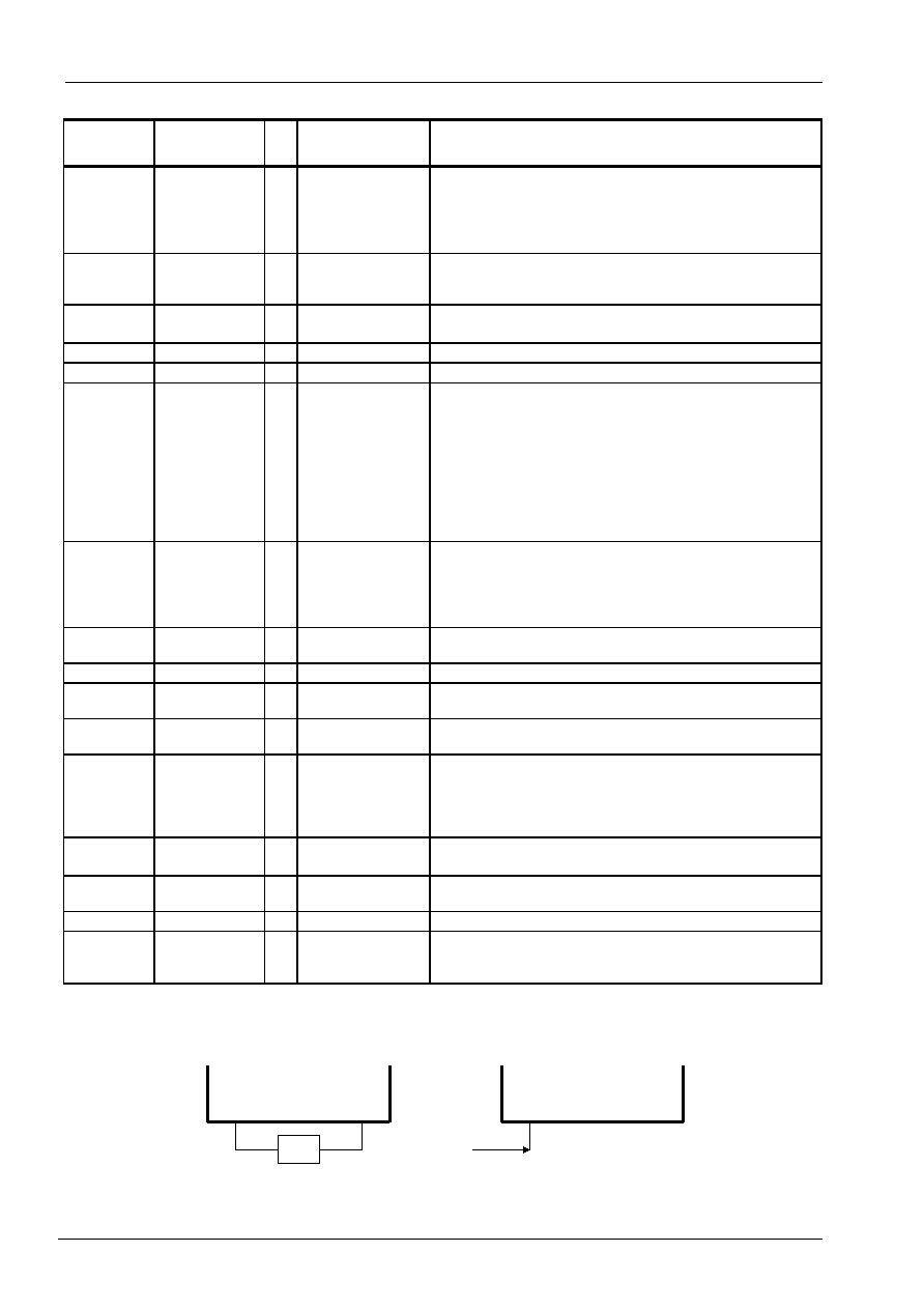
Instructions
There are four categories of instructions that:
Designate ST7070 functions, such as display format, data length, etc.
Set internal RAM addresses
Perform data transfer with internal RAM
Others
Instruction Table:
Instruction Code
Instruction
RS R/W DB7 DB6 DB5 DB4 DB3 DB2 DB1 DB0
Description
Description
Time
(270KHz)
EXT = 0 or 1
Clear
Display
0
0 0 0 0 0 0 0 0 1
Write "20H" to DDRAM. and
set DDRAM address to
"00H" from AC
1.52 ms
Return
Home
0
0 0 0 0 0 0 0 1 x
Set DDRAM address to
"00H" from AC and return
cursor to its original position
if shifted. The contents of
DDRAM are not changed.
1.52 ms
Display
ON/OFF
0
0 0 0 0 0 1 D
C
P
D=1:entire display on
C=1:cursor on
P: font table page selection
37 us
Cursor or
Display
Shift
0
0 0 0 0 1 S/C
R/L
x x
Set cursor moving and
display shift control bit, and
the direction, without
changing DDRAM data.
37 us
Function
Set
0
0 0 0 1 DL
N
EXT
x x
DL: interface data is 8/4 bits
N: number of line is 2/1
37 us
Read Busy
flag and
address
0
1 BF
AC6
AC5
AC4 AC3 AC2 AC1 AC0
Whether during internal
operation or not can be
known by reading BF. The
contents of address counter
can also be read.
0 us
Write data
to RAM
1
0 D7
D6 D5 D4
D3
D2
D1
D0
Write data into internal
RAM
(DDRAM/CGRAM)
37 us
Read data
from RAM
1
1 D7
D6 D5 D4
D3
D2
D1
D0
Read data from internal
RAM
(DDRAM/CGRAM)
37 us
EXT = 0
Entry Mode
Set
0
0 0 0 0 0 0 1 I/D
S
Sets cursor move direction
and specifies display shift.
These operations are
performed during data write
and read.
37 us
Set CGRAM
address
0
0 0 1
AC5
AC4 AC3 AC2 AC1 AC0
Set CGRAM address in
address counter
37 us
Set DDRAM
address
0
0 1
AC6
AC5
AC4 AC3 AC2 AC1 AC0
Set DDRAM address in
address counter
37 us
ST7070
V0.8
2003/11/10
16/51
EXT = 1
Bias resistor
select
0
0 0 0 0 0 0 1
Rb1 Rb0
Used internal resister only
provide 1/5 bias mode .
Rb[1:0]=00 External
Resister
Rb[1:0]=01~11 Internal
Resistor
37 us
COM
SEG
direction
select
0
0 0 1 0 0 C1
C2
S1
S2
C1
com1~8 com8~1
C2
com9~16 com16~9
S1
seg1~40 seg40~1
S2
seg41~80 seg80~41
37 us
Set display
data length
0
0 1 L6 L5
L4
L3
L2
L1
L0
To specify the number of
data bytes(3SPI mode)
37 us
Note:
Be sure the ST7070 is not in the busy state (BF = 0) before sending an instruction from the MPU to the ST7070. If an
instruction is sent without checking the busy flag, the time between the first instruction and next instruction will take
much longer than the instruction time itself. Refer to Instruction Table for the list of each instruction execution time.

ST7070
V0.8
2003/11/10
17/51
Instruction Description
EXT=0 or 1
Clear
Display
Clear all the display data by writing "20H" (space code) to all DDRAM address, and set DDRAM address to "00H"
into AC (address counter). Return cursor to the original status, namely, bring the cursor to the left edge on first line
of the display. Make entry mode increment (I/D = "1").
Return
Home
Return Home is cursor return home instruction. Set DDRAM address to "00H" into the address counter. Return
cursor to its original site and return display to its original status, if shifted. Contents of DDRAM does not change.
Display
ON/OFF
Control display/cursor/blink ON/OFF 1 bit register.
D : Display ON/OFF control bit
When D = "High", entire display is turned on.
When D = "Low", display is turned off, but display data is remained in DDRAM.
C : Cursor ON/OFF control bit
When C = "High", cursor is turned on.
When C = "Low", cursor is disappeared in current display, but I/D register remains its data.
P : Font table selection bit
When P = "Low", it select page 1 of font table.(set DDRAM data bit-8=0)
When P = "High", it select page 2 of font table(set DDRAM data bit-8=1)
0
0
0
0
0
0
0
0
0
0
0
0
0
0
0
0
0
0
0
0
1
0
0
D
Code
Code
Code
RS
RS
RS
RW
RW
RW
DB7
DB7
DB7
DB6
DB6
DB6
DB5
DB5
DB5
DB4
DB4
DB4
DB1
DB1
DB1
DB2
DB2
DB2
DB3
DB3
DB3
0
1
C
1
x
P
DB0
DB0
DB0
Every
32 frames
Alternating
display
Cursor
ST7070
V0.8
2003/11/10
18/51
Cursor or Display Shift
Without writing or reading of display data, shift right/left cursor position or display. This instruction is used to correct
or search display data. During 2-line mode display, cursor moves to the 2nd line after 40th digit of 1st line. Note that
display shift is performed simultaneously in all the line. When displayed data is shifted repeatedly, each line shifted
individually. When display shift is performed, the contents of address counter are not changed.
S/C R/L
Description
AC
Value
L
L
Shift cursor to the left
AC=AC-1
L
H
Shift cursor to the right
AC=AC+1
H
L
Shift display to the left. Cursor follows the display shift
AC=AC
H
H
Shift display to the right. Cursor follows the display shift AC=AC
Function
Set
DL : Interface data length control bit
When DL = "High", it means 8-bit bus mode with MPU.
When DL = "Low", it means 4-bit bus mode with MPU. So to speak, DL is a signal to select
8-bit or 4-bit bus mode.
When 4-bit bus mode, it needs to transfer 4-bit data by two times.
N : Display line number control bit
When N = "Low", it means 1-line display mode.
When N = "High", 2-line display mode is set.
EXT : Select basic or extended instruction set
When EXT="L" the commands `Entry Mode Set' , `Set CGRAM address' and `Set DDRAM address' can be
performed , when EXT="H" the commands `Bias resistor select' , `COM
SEG direction select' and `Set display
data length' can be performed. Other command can be executed in both cases.
When EXT="L" : disable extension instruction
When EXT="H" : enable extension instruction
0
0
0
0
0
1
S/C R/L
Code
RS
RW
DB7
DB6 DB5 DB4
DB1
DB2
DB3
x
x
DB0
0
0
0
0
1
DL
N
EXT
Code
RS
RW
DB7
DB6
DB5 DB4
DB1
DB2
DB3
x
x
DB0

ST7070
V0.8
2003/11/10
19/51
Read Busy Flag and Address
When BF = "High", indicates that the internal operation is being processed.So during this time the next
instruction cannot be accepted.
The address Counter (AC) stores DDRAM/CGRAM addresses, transferred from IR.
After writing into (reading from) DDRAM/CGRAM, AC is automatically increased (decreased) by 1.
Write Data to CGRAM or DDRAM
Write binary 8-bit data to DDRAM/CGRAM.
The selection of RAM from DDRAM, CGRAM, is set by the previous address set instruction
: DDRAM address set, CGRAM address set. RAM set instruction can also determine the AC
direction to RAM. DDRAM data bit-8 is come from "P"(Display on/off instruction) register setting
After write operation, the address is automatically increased/decreased by 1, according to
the entry mode.
Read Data from CGRAM or DDRAM
Read binary 8-bit data from DDRAM/CGRAM.
The selection of RAM is set by the previous address set instruction. If address set instruction of RAM is not
performed before this instruction, the data that read first is invalid, because the direction of AC is not determined. If
you read RAM data several times without RAM address set instruction before read operation, you can get correct
RAM data from the second, but the first data would be incorrect, because there is no time margin to transfer RAM
data.
In case of DDRAM read operation, cursor shift instruction plays the same role as DDRAM address
set instruction : it also transfer RAM data to output data register. After read operation address counter is
automatically increased/decreased by 1 according to the entry mode. After CGRAM read operation, display shift
may not be executed correctly.
* In case of RAM write operation, after this AC is increased/decreased by 1 like read operation. In this time, AC
indicates the next address position, but you can read only the previous data by read instruction.
1
1
0
1
D7
D7
D6
D6
D5
D5
D4
D4
D3
D3
D2
D2
Code
Code
RS
RS
RW
RW
DB7
DB7
DB6
DB6
DB5
DB5
DB4
DB4
DB1
DB1
DB2
DB2
DB3
DB3
D1
D1
D0
D0
DB0
DB0
0
1
BF
AC6 AC5 AC4 AC3 AC2
Code
RS
RW
DB7
DB6
DB5
DB4
DB1
DB2
DB3
AC1 AC0
DB0

ST7070
V0.8
2003/11/10
20/51
EXT=0
Entry Mode Set
Set the moving direction of cursor and display.
I/D : Increment / decrement of DDRAM address (cursor or blink)
When I/D = "High", cursor moves to right and DDRAM address is increased by 1.
When I/D = "Low", cursor moves to left and DDRAM address is decreased by 1.
* CGRAM operates the same as DDRAM, when read from or write to CGRAM.
S: Shift of entire display
When DDRAM read (CGRAM read/write) operation or S = "Low", shift of entire display is not performed. If S =
"High" and DDRAM write operation, shift of entire display is performed according to I/D value (I/D = "1" : shift
left, I/D = "0" : shift right).
S I/D
Description
H
H
Shift the display to the left
H
L
Shift the display to the right
Set CGRAM Address
Set CGRAM address to AC.
This instruction makes CGRAM data available from MPU.
Set DDRAM Address
Set DDRAM address to AC.
This instruction makes DDRAM data available from MPU.
When 1-line display mode (N = 0), DDRAM address is from "00H" to "4FH".
In 2-line display mode (N = 1), DDRAM address in the 1st line is from "00H" to "27H", and
DDRAM address in the 2nd line is from "40H" to "67H".
0
0
1
AC6
AC5
AC4 AC3 AC2
Code
RS
RW
DB7
DB6
DB5
DB4
DB1
DB2
DB3
AC1 AC0
DB0
0
0
0
1
AC5 AC4 AC3 AC2
Code
RS
RW
DB7
DB6
DB5
DB4
DB1
DB2
DB3
AC1 AC0
DB0
0
0
0
0
0
0
0
1
Code
RS
RW
DB7
DB6 DB5 DB4
DB1
DB2
DB3
I/D
S
DB0
ST7070
V0.8
2003/11/10
21/51
EXT=1
Bias resistor select
Set internal bias resistor value.
Rb1 Rb0
Description
L
L
External bias resistor select.
L
H
Build-in resistor select (R=2.2K).
H
L
Build-in resistor select (R=6.8K).
H H
Build-in resistor select (R=9.0K).
COM
SEG direction select
The SEG and COM output in ST7070 all have bi-direction control by the register.
COM OUTPUT :
COM output
C1
COM1 COM8
0 COM1
Common Address COM8
1 COM8
Common Address COM1
COM output
C2
COM9 COM16
0 COM9
Common Address COM16
1 COM16
Common Address COM9
SEG OUTPUT :
SEG output
S1
SEG1 SEG40
0
SEG1 Segment Address SEG40
1 SEG40
Segment Address SEG1
SEG output
S2
SEG41 SEG80
0
SEG41 Segment Address SEG80
1
SEG80 Segment Address SEG41
0
0
0
0
0
0
0
1
Code
RS
RW
DB7
DB6
DB5
DB4
DB1
DB2
DB3
Rb1 Rb0
DB0
0
0
0
1
0
0
C1
C2
Code
RS
RW
DB7
DB6
DB5
DB4
DB1
DB2
DB3
S1
S2
DB0
ST7070
V0.8
2003/11/10
22/51
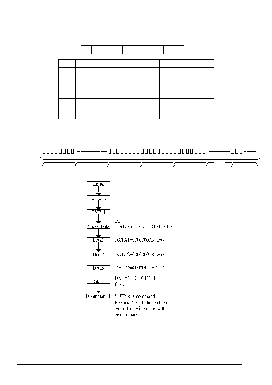
Set display data length
L6 L5 L4 L3 L2 L1 L0 Data
length
0 0 0 0 0 0 0
1
0 0 0 0 0 0 1
2
.... ... ... ... ... ... ....
...
1 0 0 1 1 1 0
79
1 0 0 1 1 1 1
80
Only in 3line-SPI interface will use the register to set the number of display data(Max=4F).
To write data to DDRAM , send Data Direction Command in 3-pin SPI . Data is latched at the rising edge of SCLK .
And the DDRAM column address pointer will be increased by one automatically.
initial
EXT=1
No.of Data
Data0
Command
SCLK
SDI
CSB
0
0
0
1
L5
L4
L3
L2
Code
RS
RW
DB7
DB6
DB5
DB4
DB1
DB2
DB3
L1
L0
DB0

ST7070
V0.8
2003/11/10
23/51
Reset Function
Initializing by Internal Reset Circuit
An internal reset circuit automatically initializes the ST7070 when the power is turned on or hardware reset pin has
low. The following instructions are executed during the initialization. The busy flag (BF) is kept in the busy state until
the initialization ends (BF = 1). The busy state lasts for 40 ms after VCC rises to 4.5 V.
1. Display clear
2. Function set:
DL = 1; 8-bit interface data
N = 1; 2-line display
EXT=0;disable extension instruction.
3. Display on/off control:
D = 0; Display off
C = 0; Cursor off
P = 0; Page 1 of font table(DDRAM data b8=0)
4. Entry mode set:
I/D = 1; Increment by 1
S = 0; No shift
5. Bias resistor select:
Rb1=0;Rb2=0 select external bias resistor.
6. COM
SEG direction select:
C1=0;C2=0;S1=0;S2=0 not reverse.
Note:
If the electrical characteristics conditions listed under the table Power Supply Conditions Using
Internal Reset Circuit are not met, the internal reset circuit will not operate normally and will fail
to initialize the ST7070. For such a case, initialization must be performed by the MPU as
explain by the following figure.

ST7070
V0.8
2003/11/10
24/51
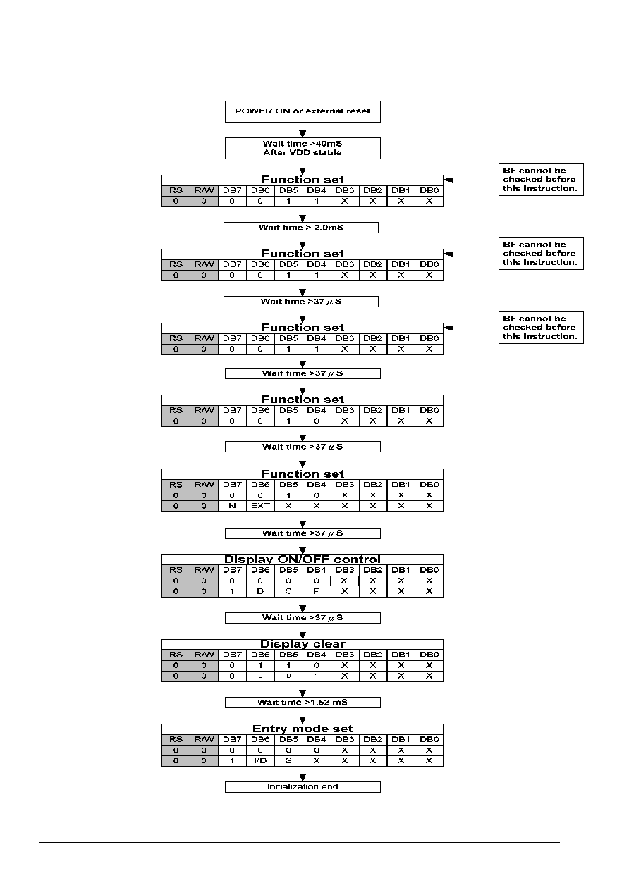
Initializing by Instruction
8-bit Interface (fosc=270KHz)
POWER ON
Wait time >40mS
After Vcc >4.5V
Function set
RS R/W DB7 DB6 DB5 DB4 DB3 DB2 DB1 DB0
0 0 0 0
1
1
N
X
X
X
Wait time >37uS
Function set
RS R/W DB7 DB6 DB5 DB4 DB3 DB2 DB1 DB0
0 0 0 0
1
1
N
X
X
X
Wait time >37uS
Display ON/OFF control
RS R/W DB7 DB6 DB5 DB4 DB3 DB2 DB1 DB0
0 0 0 0
0
0
1
D
C
P
Wait time >37uS
Display clear
RS R/W DB7 DB6 DB5 DB4 DB3 DB2 DB1 DB0
0
0
0
0
0
0
0
0
0
1
Wait time >1.52mS
Entry mode set
RS R/W DB7 DB6 DB5 DB4 DB3 DB2 DB1 DB0
0 0 0 0
0
0
0
1
I/D
S
Initialization end
BF cannot be
checked before
this instruction.
BF cannot be
checked before
this instruction.

ST7070
V0.8
2003/11/10
25/51
Initial Program Code Example For 8051 MPU(8 Bit Interface):
;---------------------------------------------------------------------------------
INITIAL_START:
CALL DELAY40mS
MOV A,#38H ;FUNCTION SET
CALL WRINS_NOCHK ;8 bit,N=1,5*7dot
CALL DELAY37uS
MOV A,#38H ;FUNCTION SET
CALL WRINS_NOCHK ;8 bit,N=1,5*7dot
CALL DELAY37uS
MOV A,#0FH ;DISPLAY ON
CALL WRINS_CHK
CALL DELAY37uS
MOV A,#01H ;CLEAR DISPLAY
CALL WRINS_CHK
CALL DELAY1.52mS
MOV A,#06H ;ENTRY MODE SET
CALL WRINS_CHK ;CURSOR MOVES TO RIGHT
CALL DELAY37uS
;---------------------------------------------------------------------------------
MAIN_START:
XXXX
XXXX
XXXX
XXXX
.
.
.
.
;---------------------------------------------------------------------------------
WRINS_CHK:
CALL CHK_BUSY
WRINS_NOCHK:
CLR RS
;EX:Port 3.0
CLR RW
;EX:Port 3.1
SETB E
;EX:Port 3.2
MOV P1,A
;EX:Port 1=Data Bus
CLR E
MOV P1,#FFH
;For Check Busy Flag
RET
;---------------------------------------------------------------------------------
CHK_BUSY:
;Check
Busy
Flag
CLR RS
SETB RW
SETB E
JB P1.7,$
CLR E
RET
ST7070
V0.8
2003/11/10
26/51
4-bit Interface (fosc=270KHz)

ST7070
V0.8
2003/11/10
27/51
Initial Program Code Example For 8051 MPU(4 Bit Interface):
;-------------------------------------------------------------------
INITIAL_START:
CALL DELAY40mS
MOV A,#38H ;FUNCTION SET
CALL WRINS_ONCE ;8 bit,N=1,5*7dot
CALL DELAY2mS
MOV A,#38H ;FUNCTION SET
CALL WRINS_ONCE ;8 bit,N=1,5*7dot
CALL DELAY37uS
MOV A,#38H ;FUNCTION SET
CALL WRINS_ONCE ;8 bit,N=1,5*7dot
CALL DELAY37uS
MOV A,#28H ;FUNCTION SET
CALL WRINS_NOCHK ;4 bit,N=1,5*7dot
CALL DELAY37uS
MOV A,#28H ;FUNCTION SET
CALL WRINS_NOCHK ;4 bit,N=1,5*7dot
CALL DELAY37uS
MOV A,#0FH ;DISPLAY ON
CALL WRINS_CHK
CALL DELAY37uS
MOV A,#01H ;CLEAR DISPLAY
CALL WRINS_CHK
CALL DELAY1.52mS
MOV A,#06H ;ENTRY MODE SET
CALL WRINS_CHK
CALL DELAY37uS
;-------------------------------------------------------------------
MAIN_START:
XXXX
XXXX
XXXX
XXXX
.
.
.
.
.
.
.
.
.
;-------------------------------------------------------------------
WRINS_CHK:
CALL CHK_BUSY
WRINS_NOCHK:
PUSH A
ANL A,#F0H
CLR RS
;EX:Port 3.0
CLR RW
;EX:Port 3.1
SETB E
;EX:Port 3.2
MOV P1,A
;EX:Port1=Data Bus
CLR E
POP A
SWAP A
WRINS_ONCE:
ANL A,#F0H
CLR RS
CLR RW
SETB E
MOV P1,A
CLR E
MOV P1,#FFH
;For Check Bus Flag
RET
;-------------------------------------------------------------------
CHK_BUSY:
;Check
Busy
Flag
PUSH A
MOV P1,#FFH
$1
CLR RS
SETB RW
SETB E
MOV A,P1
CLR E
MOV P1,#FFH
CLR RS
SETB RW
SETB E
NOP
CLR E
JB A.7,$1
POP A
RET
ST7070
V0.8
2003/11/10
28/51
Serial Interface (fosc=270KHz)
POWER ON
Wait time >40mS
After Vcc >4.5V
Function set
RS R/W DB7 DB6 DB5 DB4 DB3 DB2 DB1 DB0
0 0 0 0
1
X
N
X
X
X
Wait time >37uS
Display ON/OFF control
RS R/W DB7 DB6 DB5 DB4 DB3 DB2 DB1 DB0
0 0 0 0
0
0
1
D
C
P
Wait time >37uS
Display clear
RS R/W DB7 DB6 DB5 DB4 DB3 DB2 DB1 DB0
0
0
0
0
0
0
0
0
0
1
Wait time >1.52mS
Entry mode set
RS R/W DB7 DB6 DB5 DB4 DB3 DB2 DB1 DB0
0 0 0 0
0
0
0
1
I/D
S
Initialization end
BF cannot be
checked before
this instruction.

ST7070
V0.8
2003/11/10
29/51
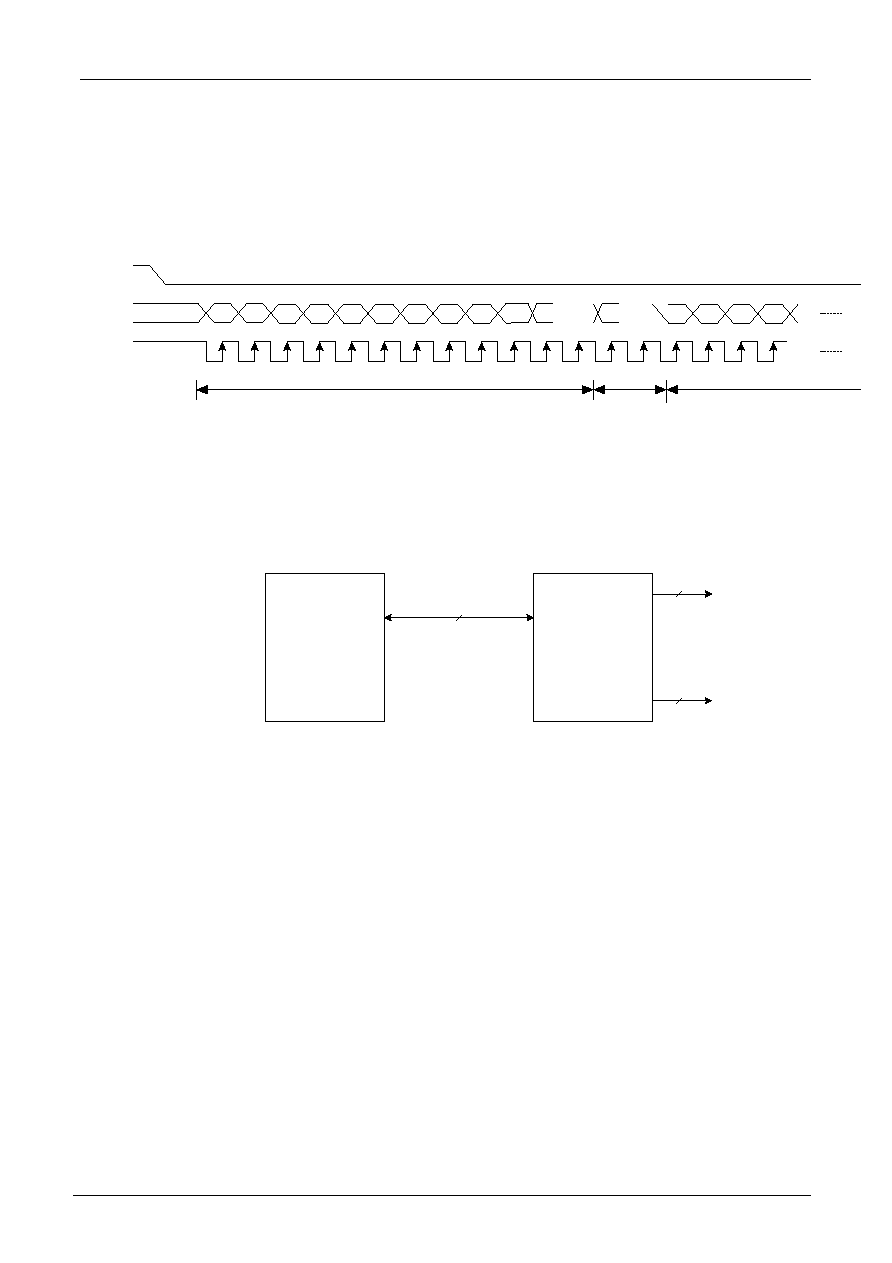
Interfacing to the MPU
The ST7070 can send data in either two 4-bit operations or one 8-bit operation or serial operation, thus allowing
interfacing with 4- or 8-bit or serial MPU.
For 4-bit interface data, only four bus lines (DB4 to DB7) are used for transfer. Bus lines DB0 to DB3
are disabled. The data transfer between the ST7070 and the MPU is completed after the 4-bit data has been
transferred twice. As for the order of data transfer, the four high order bits (for 8-bit operation, DB4 to DB7)
are transferred before the four low order bits (for 8-bit operation, DB0 to DB3). The busy flag must be
checked (one instruction) after the 4-bit data has been transferred twice. Two more 4-bit operations then
transfer the busy flag and address counter data.
Example of busy flag check timing sequence
Intel 8051 interface
P1.0 to P1.3
P3.0
P3.1
P3.2
RS
R/W
E
DB4 to DB7
COM1 to COM16
SEG1 to SEG80
80
16
Intel 8051 Serial
ST7070
4
Functioning
DB7
Internal
operation
E
R/W
RS
Busy flag check
Busy flag check
Instruction write
Instruction write
IR7
IR3
AC
3
Not
Busy
AC
3
IR3
IR7

ST7070
V0.8
2003/11/10
30/51
For 8-bit interface data, all eight bus lines (DB0 to DB7) are used.
Example of busy flag check timing sequence
Intel 8051 interface
Data
Not
Busy
Busy
Busy
Data
Functioning
DB7
Internal
operation
E
R/W
RS
Busy flag
check
Busy flag
check
Busy flag
check
Instruction
write
Instruction
write
P1.0 to P1.7
P3.0
P3.1
P3.2
RS
R/W
E
DB0 to DB7
COM1 to COM16
SEG1 to SEG80
80
16
Intel 8051 Serial
ST7070
8
ST7070
V0.8
2003/11/10
31/51
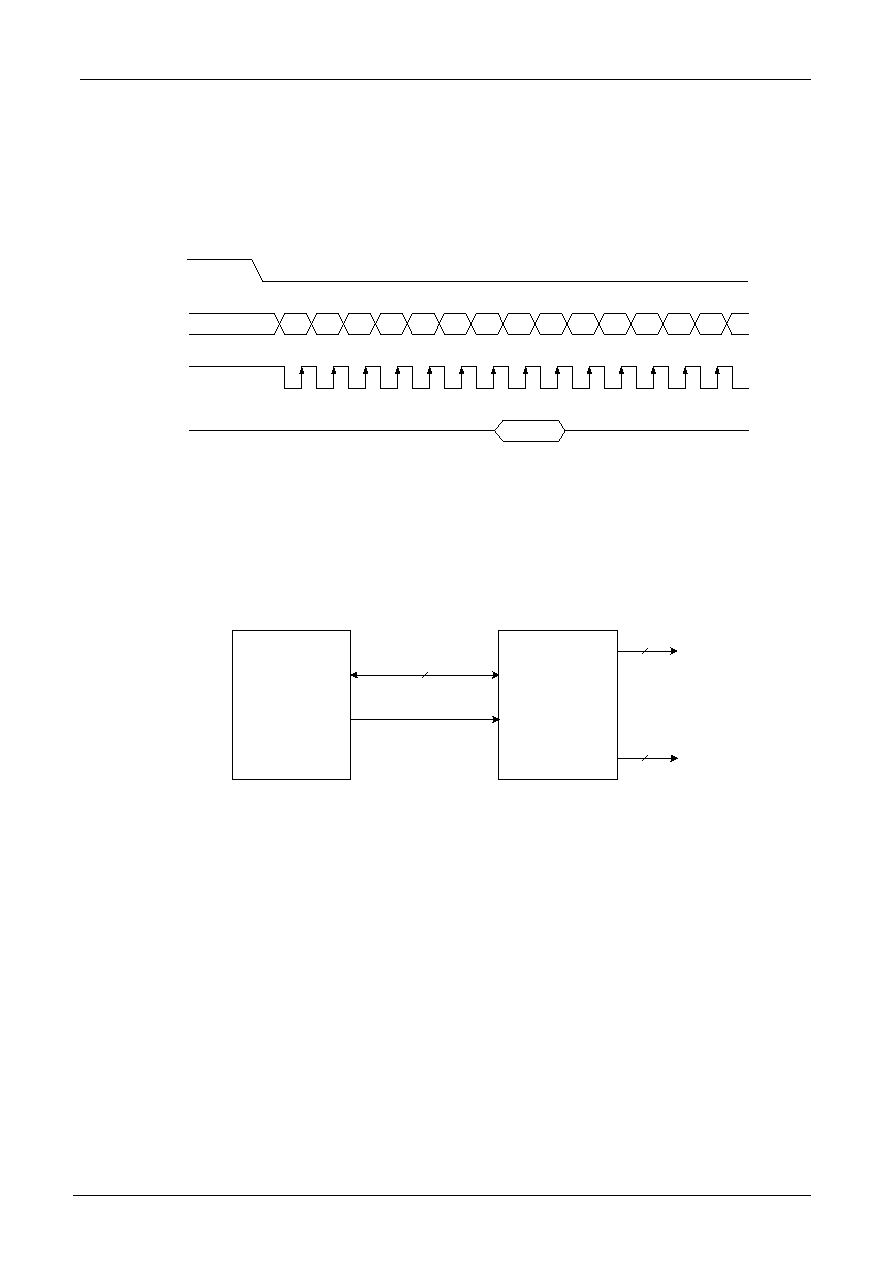
For serial interface data, bus lines (DB5 to DB7) are used. 4-Pin SPI
Example of timing sequence
Intel 8051 interface(Serial)
1
2
3
4
5
6
7
8
9
10
11
12
13
14
D7
D6
D5
D4
D3
D2
D1
D0
D7
D6
D5
D4
D3
D2
CSB
SI
SCL
RS
P1.5to P1.7
P3.0
RS
SI , SCL , /CS
COM1 to COM16
SEG1 to SEG80
80
16
Intel 8051 Serial
ST7070
3
ST7070
V0.8
2003/11/10
32/51
For serial interface data, bus lines (DB5 to DB7) are used. 3-Pin SPI
Example of timing sequence
DB7
DB6
DB5
DB4
DB3
DB2
DB1
DB0
DB7
DB6
/CB
SI
SCL
DB7
DB6
DB5
DB4
DB3
display data
length
set command
number of
data
set data
Intel 8051 interface(Serial)
P1.5to P1.7
SI , SCL , /CS
COM1 to COM16
SEG1 to SEG80
80
16
Intel 8051 Serial
ST7070
3

ST7070
V0.8
2003/11/10
33/51
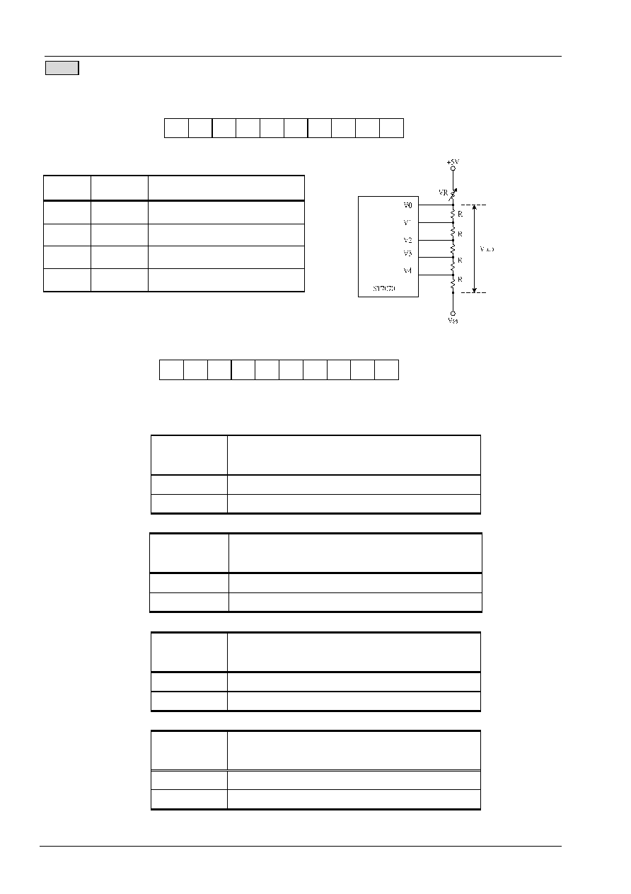
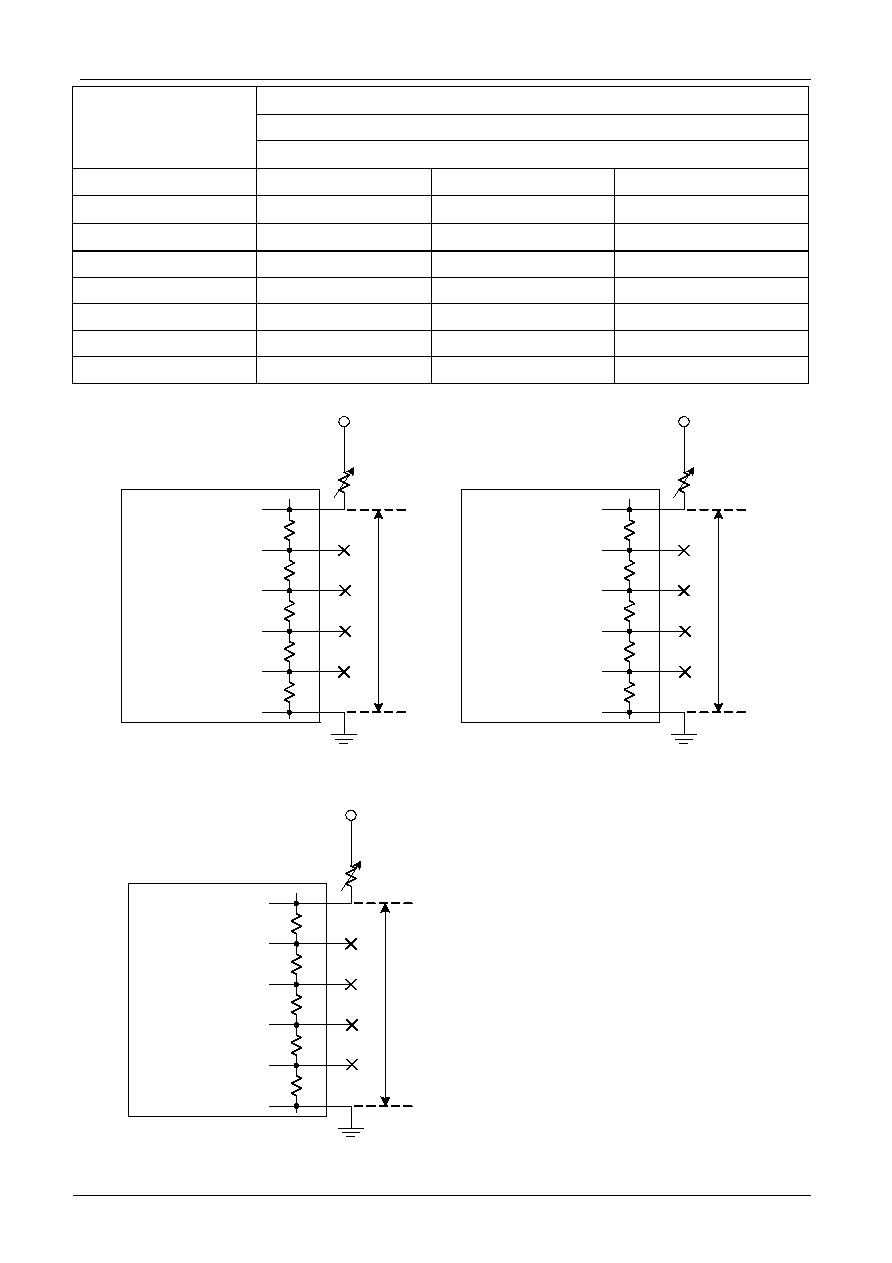
Supply Voltage for LCD Drive
There are different voltages that supply to ST7070's pin (V0 � V4) to obtain LCD drive waveform. We could use
the register command (Ra1,Ra0) to set up the Internal or External Bias Resister. The relations of the bias, duty
factor and supply voltages are shown as below. External Bias Resistor could set up to 1/4 bias and 1/5 bias,
but Internal Bias Resistor only could set up to 1/5 bias.
Duty Factor
1/8 1/8,1/16
External
Resistor
Bias
Supply Voltage
1/4 1/5
Bias Resistor Select
Ra1=0,Ra0=0 Ra1=0,Ra0=0
V0 VLCD
VLCD
V1 3/4VLCD 4/5VLCD
V2 1/2VLCD 3/5VLCD
V3 1/2VLCD 2/5VLCD
V4 1/4VLCD 1/5VLCD
1/4 bias
(1/8 duty cycle)
V0
V1
V2
V3
V4
VR
+5V
V
LCD
R
R
R
R
Vss
VR
+5V
V
LCD
R
R
R
R
Vss
V0
V1
V2
V3
V4
1/5 bias
(1/16 duty cycle)
R
ST7070
V0.8
2003/11/10
34/51
Duty Factor
1/8 , 1/16
Internal
Resistor
Bias
Supply Voltage
1/5 1/5 1/5
Bias Resistor Select
Ra1=0,Ra0=1 Ra1=1,Ra0=0 Ra1=1,Ra0=1
Internal Resistor
R=2.2K R=6.8K R=9.0K
V0
VLCD
VLCD
VLCD
V1 4/5VLCD
4/5VLCD
4/5VLCD
V2 3/5VLCD
3/5VLCD
3/5VLCD
V3 2/5VLCD
2/5VLCD
2/5VLCD
V4 1/5VLCD
1/5VLCD
1/5VLCD
VR
+5V
V
LCD
R
R
R
R
GND
V0
V1
V2
V3
V4
1/5 bias R=2.2K
(1/8,1/16 duty cycle)
VSS
VR
+5V
V
LCD
R
R
R
R
GND
V0
V1
V2
V3
V4
VSS
1/5 bias R=6.8K
(1/8,1/16 duty cycle)
Ra1=0,Ra0=1
Ra1=1,Ra0=0
R
R
VR
+5V
V
LCD
R
R
R
R
GND
V0
V1
V2
V3
V4
1/5 bias R=9.0K
(1/8,1/16 duty cycle)
VSS
R
Ra1=1,Ra0=1

ST7070
V0.8
2003/11/10
35/51
Timing Characteristics
Writing data from MPU to ST7070
Reading data from ST7070 to MPU
VIH1
VIL1
t
AS
t
AH
t
PW
t
AH
t
DSW
t
H
t
C
t
r
t
f
Valid data
RS
E
RW
DB0-DB7
VIH1
VIL1
t
AS
t
AH
t
PW
t
AH
t
H
t
C
t
r
t
f
Valid data
RS
E
RW
DB0-DB7
t
DDR

ST7070
V0.8
2003/11/10
36/51
V
OH2
V
OL2
t
CWH
t
CST
t
CWH
t
CWL
t
ct
t
DH
t
SU
t
DM
CL1
CL2
D
M
t
ct
2.7V/4.5V
0.2V
0.2V
0.2V
t
rcc
t
OFF
t
OFF
1mS
0.1mStrcc80mS
Notes:
t
OFF
compensates for the power oscillation period caused by momentary power supply oscillations.
Specified at 4.5V for 5V operation,and at 2.7V for 3V operation.
For if 4.5V is not reached during 5V operation,teh internal reset circuit will not operate normally.
Interface Timing with External Driver
Internal Power Supply Reset

ST7070
V0.8
2003/11/10
37/51
AC Characteristics
In 6800 interface
(TA = 25
, VCC = 2.7V )
Symbol Characteristics
Test
Condition Min. Typ. Max. Unit
Internal Clock Operation
f
OSC
OSC Frequency
R = 75K
190 270 350 KHz
External Clock Operation
f
EX
External
Frequency
-
125 270 410 KHz
Duty
Cycle
-
45 50 55 %
T
R
,T
F
Rise/Fall
Time
-
- - 0.2
�
s
Write Mode (Writing data from MPU to ST7070)
T
C
Enable Cycle Time Pin E
40
-
-
us
T
PW
Enable Pulse Width Pin E
40
-
-
ns
T
R
,T
F
Enable Rise/Fall Time Pin E
-
-
25
ns
T
AS
Address Setup Time Pins: RS,RW,E
0
-
-
ns
T
AH
Address Hold Time Pins: RS,RW,E
10
-
-
ns
T
DSW
Data Setup Time
Pins: DB0 - DB7
20
-
-
ns
T
H
Data Hold Time
Pins: DB0 - DB7
10
-
-
ns
Read Mode (Reading Data from ST7070 to MPU)
T
C
Enable Cycle Time Pin E
1200
-
-
ns
T
PW
Enable Pulse Width Pin E
480
-
-
ns
T
R
,T
F
Enable Rise/Fall Time Pin E
-
-
25
ns
T
AS
Address Setup Time Pins: RS,RW,E
0
-
-
ns
T
AH
Address Hold Time Pins: RS,RW,E
10
-
-
ns
T
DDR
Data Setup Time
Pins: DB0 - DB7
-
-
320
ns
T
H
Data Hold Time
Pins: DB0 - DB7
10
-
-
ns
Interface Mode with LCD Driver(ST7921)
T
CWH
Clock Pulse with High Pins: CL1, CL2
800
-
-
ns
T
CWL
Clock Pulse with Low Pins: CL1, CL2
800
-
-
ns
T
CST
Clock Setup Time Pins: CL1, CL2
500
-
-
ns
T
SU
Data Setup Time
Pin: D
300
-
-
ns
T
DH
Data Hold Time
Pin: D
300
-
-
ns
T
DM
M Delay Time
Pin: M
0
-
2000
ns

ST7070
V0.8
2003/11/10
38/51
AC Characteristics
In 6800 interface
(TA = 25
, VCC = 5V)
Symbol Characteristics
Test
Condition Min. Typ. Max. Unit
Internal Clock Operation
f
OSC
OSC Frequency
R = 91K
190
270
350
KHz
External Clock Operation
f
EX
External
Frequency
-
125
270
410 KHz
Duty
Cycle
-
45
50
55
%
T
R
,T
F
Rise/Fall
Time
-
- - 0.2
�
s
Write Mode (Writing data from MPU to ST7070)
T
C
Enable Cycle Time Pin E
20
-
-
us
T
PW
Enable Pulse Width Pin E
40
-
-
ns
T
R
,T
F
Enable Rise/Fall Time Pin E
-
-
25
ns
T
AS
Address Setup Time Pins: RS,RW,E
0
-
-
ns
T
AH
Address Hold Time Pins: RS,RW,E
10
-
-
ns
T
DSW
Data Setup Time
Pins: DB0 - DB7
20
-
-
ns
T
H
Data Hold Time
Pins: DB0 - DB7
10
-
-
ns
Read Mode (Reading Data from ST7070 to MPU)
T
C
Enable Cycle Time Pin E
1200
-
-
ns
T
PW
Enable Pulse Width Pin E
140
-
-
ns
T
R
,T
F
Enable Rise/Fall Time Pin E
-
-
25
ns
T
AS
Address Setup Time Pins: RS,RW,E
0
-
-
ns
T
AH
Address Hold Time Pins: RS,RW,E
10
-
-
ns
T
DDR
Data Setup Time
Pins: DB0 - DB7
-
-
100
ns
T
H
Data Hold Time
Pins: DB0 - DB7
10
-
-
ns
Interface Mode with LCD Driver(ST7921)
T
CWH
Clock Pulse with High Pins: CL1, CL2
800
-
-
ns
T
CWL
Clock Pulse with Low Pins: CL1, CL2
800
-
-
ns
T
CST
Clock Setup Time Pins: CL1, CL2
500
-
-
ns
T
SU
Data Setup Time
Pin: D
300
-
-
ns
T
DH
Data Hold Time
Pin: D
300
-
-
ns
T
DM
M Delay Time
Pin: M
0
-
2000
ns

ST7070
V0.8
2003/11/10
39/51
AC Characteristics
In Serial interface
(TA = 25
, VCC = 2.7V )
Symbol Characteristics
Test
Condition Min. Typ. Max. Unit
Internal Clock Operation
f
OSC
OSC Frequency
R = 75K
190 270 350 KHz
External Clock Operation
f
EX
External
Frequency
-
125 270 410 KHz
Duty
Cycle
-
45 50 55 %
T
R
,T
F
Rise/Fall
Time
-
- - 0.2
�
s
Write Mode (Writing data from MPU to ST7070)
T
C
Enable Cycle Time Pin E
2000
-
-
ns
T
PW
Enable Pulse Width Pin E
950
-
-
ns
T
R
,T
F
Enable Rise/Fall Time Pin E
-
-
25
ns
T
AS
Address Setup Time Pins: RS,E
50
-
-
ns
T
AH
Address Hold Time Pins: RS,,E
10
-
-
ns
T
DSW
Data Setup Time
Pins: DB0 - DB7
10
-
-
ns
T
H
Data Hold Time
Pins: DB0 - DB7
50
-
-
ns
Interface Mode with LCD Driver(ST7921)
T
CWH
Clock Pulse with High Pins: CL1, CL2
800
-
-
ns
T
CWL
Clock Pulse with Low Pins: CL1, CL2
800
-
-
ns
T
CST
Clock Setup Time Pins: CL1, CL2
500
-
-
ns
T
SU
Data Setup Time
Pin: D
300
-
-
ns
T
DH
Data Hold Time
Pin: D
300
-
-
ns
T
DM
M Delay Time
Pin: M
0
-
2000
ns
ST7070
V0.8
2003/11/10
40/51
AC Characteristics
In Serial Interface
(TA = 25
, VCC = 5V)
Symbol Characteristics
Test
Condition Min. Typ.
Max. Unit
Internal Clock Operation
f
OSC
OSC Frequency
R = 91K
190
270
350
KHz
External Clock Operation
f
EX
External
Frequency
-
125
270
410 KHz
Duty
Cycle
-
45
50
55
%
T
R
,T
F
Rise/Fall
Time
-
- - 0.2
�
s
Write Mode (Writing data from MPU to ST7070)
T
C
Enable Cycle Time Pin E
800
-
-
ns
T
PW
Enable Pulse Width Pin E
40
-
-
ns
T
R
,T
F
Enable Rise/Fall Time Pin E
-
-
25
ns
T
AS
Address Setup Time Pins: RS,E
50
-
-
ns
T
AH
Address Hold Time Pins: RS,E
10
-
-
ns
T
DSW
Data Setup Time
Pins: DB0 - DB7
10
-
-
ns
T
H
Data Hold Time
Pins: DB0 - DB7
50
-
-
ns
Interface Mode with LCD Driver(ST7921)
T
CWH
Clock Pulse with High Pins: CL1, CL2
800
-
-
ns
T
CWL
Clock Pulse with Low Pins: CL1, CL2
800
-
-
ns
T
CST
Clock Setup Time Pins: CL1, CL2
500
-
-
ns
T
SU
Data Setup Time
Pin: D
300
-
-
ns
T
DH
Data Hold Time
Pin: D
300
-
-
ns
T
DM
M Delay Time
Pin: M
0
-
2000
ns

ST7070
V0.8
2003/11/10
41/51
Absolute Maximum Ratings
Characteristics Symbol
Value
Power Supply Voltage
V
CC
-0.3 to +5.5
LCD Driver Voltage
V
LCD
Vss+7.0 to Vss-0.3
Input Voltage
V
IN
-0.3 to V
CC
+0.3
Operating Temperature
T
A
-40
o
C to + 90
o
C
Storage Temperature
T
STO
-55
o
C to + 125
o
C
DC Characteristics
( TA = 25
, VCC = 2.7 V � 4.5 V )
Symbol
Characteristics Test
Condition Min. Typ. Max.
Unit
V
CC
Operating
Voltage
-
2.7 - 4.5 V
V
LCD
LCD Voltage
V0 - Vss
3.0
-
7.0
V
I
CC
Power
Supply
Current
f
OSC
= 270KHz
V
CC
=3.0V
- 0.1
0.25 mA
V
IH1
Input High Voltage
(Except OSC1)
- 0.7Vcc
-
V
CC
V
V
IL1
Input Low Voltage
(Except OSC1)
- -
0.3
-
0.6
V
V
IH2
Input High Voltage
(OSC1)
- 0.7Vcc
-
V
CC
V
V
IL2
Input Low Voltage
(OSC1)
- -
-
0.2Vcc
V
V
OH1
Output High Voltage
(DB0 - DB7)
I
OH
= -0.1mA
0.75
Vcc
- - V
V
OL1
Output Low Voltage
(DB0 - DB7)
I
OL
= 0.1mA
-
-
0.2Vcc
V
V
OH2
Output High Voltage
(Except DB0 - DB7)
I
OH
= -0.04mA
0.8V
CC
- V
CC
V
V
OL2
Output Low Voltage
(Except DB0 - DB7)
I
OL
= 0.04mA
-
-
0.2V
CC
V
R
COM
Common
Resistance V
LCD
= 4V, I
d
= 0.05mA
-
2
20
K
R
SEG
Segment
Resistance V
LCD
= 4V, I
d
= 0.05mA
-
2
30
K
I
LEAK
Input Leakage
Current
V
IN
= 0V to V
CC
-1
-
1
�
A
I
PUP
Pull Up MOS Current
V
CC
= 3V
10
60
120
�
A
NOTE :
External bias resistor select , so Idd doesn't include the follower current.

ST7070
V0.8
2003/11/10
42/51
DC Characteristics
( TA = 25
, V
CC
= 4.5 V - 5.5 V )
Symbol Characteristics
Test Condition Min. Typ. Max.
Unit
V
CC
Operating
Voltage
-
4.5 - 5.5 V
V
LCD
LCD Voltage
V0 - Vss
3.0
-
7.0
V
I
CC
Power Supply Current
f
OSC
= 270KHz
V
CC
=5.0V
- 0.2 0.5 mA
V
IH1
Input High Voltage
(Except OSC1)
- 2.5
-
V
CC
V
V
IL1
Input Low Voltage
(Except OSC1)
- -0.3
-
0.6
V
V
IH2
Input High Voltage
(OSC1)
- V
CC
-1
- V
CC
V
V
IL2
Input Low Voltage
(OSC1)
- -
-
1.0
V
V
OH1
Output High Voltage
(DB0 - DB7)
I
OH
= -0.1mA
3.9
-
V
CC
V
V
OL1
Output Low Voltage
(DB0 - DB7)
I
OL
= 0.1mA
-
-
0.4
V
V
OH2
Output High Voltage
(Except DB0 - DB7)
I
OH
= -0.04mA
0.9V
CC
- V
CC
V
V
OL2
Output Low Voltage
(Except DB0 - DB7)
I
OL
= 0.04mA
-
-
0.1V
CC
V
R
COM
Common
Resistance V
LCD
= 4V, I
d
= 0.05mA
-
2
20
K
R
SEG
Segment
Resistance V
LCD
= 4V, I
d
= 0.05mA
-
2
30
K
I
LEAK
Input Leakage
Current
V
IN
= 0V to V
CC
-1
-
1
�
A
I
PUP
Pull Up MOS Current
V
CC
= 5V
90
200
330
�
A
NOTE :
External bias resistor select , so Idd doesn't include the follower current.

ST7070
V0.8
2003/11/10
43/51
LCD Frame Frequency
Assume the oscillation frequency is 270KHZ, 1 clock cycle time = 3.7us, 1/16 duty; 1/5 bias,1 frame
= 3.7us x 200 x 16 = 11840us=11.8ms(84.7Hz)
1 2 3 4
16
1 2 3 4
16
1 2 3 4
16
V0
V1
V2
V3
V4
Vss
COM1
V0
V1
V2
V3
V4
Vss
COM2
V0
V1
V2
V3
V4
Vss
COM16
V0
V1
V2
V3
V4
Vss
SEGx off
V0
V1
V2
V3
V4
Vss
1 frame
SEGx on
200 clocks

ST7070
V0.8
2003/11/10
44/51
Assume the oscillation frequency is 270KHZ, 1 clock cycle time = 3.7us, 1/8 duty; 1/4 bias,1 frame =
3.7us x 400 x 8 = 11840us=11.8ms (84.7Hz)
1 2 3 4
8
1 2 3 4
8
1 2 3 4
8
V0
V1
V2
V3
V4
Vss
COM1
V0
V1
V4
Vss
COM2
V0
V1
V4
Vss
COM8
V0
V1
V4
Vss
SEGx off
V0
V1
V4
Vss
1 frame
SEGx on
V2
V3
V2
V3
V2
V3
V2
V3
400 clocks
ST7070
V0.8
2003/11/10
45/51
I/O Pad Configuration
PMOS
NMOS
PSB=1==>E(Floating)
PSB=0==>E(Pull up)
PMOS
NMOS
PSB=1==>R/W(With Pull up)
PSB=0==>R/W(With Pull down)
PMOS
NMOS
Output PAD:CL1,CL2,M,D
PMOS
V
CC
V
CC
V
CC
V
CC
NMOS
PSB
PSB
V
CC
PMOS
NMOS
PSB=1==>RS(With Pull up)
PSB=0==>RS(Floating)
PMOS
V
CC
V
CC
PSB

ST7070
V0.8
2003/11/10
46/51
PMOS
NMOS
Enable
Data
I/O PAD:DB4-DB0
PMOS
NMOS
PMOS
V
CC
V
CC
V
CC
PMOS
NMOS
Enable
Data
I/O PAD:DB7-DB5
PMOS
NMOS
PMOS
V
CC
V
CC
V
CC
PSB=1==> Pull up
PSB=0==>Pull up
PSB
PSB=1==> Pull up
PSB=0==>Floating

ST7070
V0.8
2003/11/10
47/51
LCD and ST7070 Connection
1. 5x8 dots, 16 characters x 1 line (1/4 bias, 1/8 duty)
COM1
.
.
.
.
.
.
.
.
COM8
ST7070
SEG1
.
.
.
.
.
SEG80
LCD Panel: 16 Characters x
1 line
2. 5x8 dots, 16 characters x 2 line (1/5 bias, 1/16 duty)
COM1
.
.
.
.
.
.
.
.
COM8
ST7070
SEG1
.
.
.
.
.
.
.
.
.
.
SEG80
LCD Panel: 16 Characters x
2 line
COM9
.
.
.
.
.
.
.
.
COM16
ST7070
V0.8
2003/11/10
48/51
3. 5x8 dots, 32 characters x 1 line (1/5 bias, 1/16 duty)
COM1
.
.
.
.
.
.
.
.
COM8
ST7070
SEG1
.
.
.
.
.
.
SEG80
LCD Panel: 32
Characters x 1 line
COM9
.
.
.
.
.
.
.
.
COM16

ST7070
V0.8
2003/11/10
49/51
Application Circuit
S
T
70
70
S
T
79
21
ST
79
21
Dot Matr
ix LC
D Pa
ne
l
VSS
V
cc(
+
5
V
)
Re
s
i
s
t
or
R
e
s
i
st
o
r
R
e
si
st
o
r
R
e
si
st
o
r
R
e
si
st
o
r
VR
RS/
R
W/
E
/
DB
0-DB7
To
M
P
U
V4
V3
V2
V1
V0
M
CL
1
CL
2
GND
VCC
S
e
g 1
-
80
Com
1-16
V0
VS
S
SH
L
2
SH
L
1
VC
C
DL
1
V2
V3
V2
V
3
V0
VSS
SHL
2
SHL
1
VCC
DL
1
M
CL
2
CL
1
DR1
DL
2
DR2
M
CL
2
CL
1
DR
1
DL
2
DR
2
S
e
g
1~
9
6
S
e
g
1~
24
N
ot
e:
R
e
si
st
o
r
=
2
.2
K~1
0
K o
h
m
V
R
=
1
0
K
~
3
0
K
oh
m
D
2
(
L
in
e)
X
4
0
(
C
h
ar
ac
te
r
s
)
5X8 dot
s
/
c
h
a
r
a
c
t
e
r

ST7070
V0.8
2003/11/10
50/51
THE MPU INTERFACE
The ST7070 Series can be connected to 6800 Series MPUs. Moreover, using the serial interface it is possible to
operate the ST7070 series chips with fewer signal lines.
The display area can be enlarged by using multiple ST7070 Series chips . When this is done , the chip select
signal can be used to select the individual Ics to access.
(1) 6800 8 bits Series MPUs
MPU
VCC
RS
D0 to D7
R/W
E
/RES
GND
ST7070
VDD
RS
D0 to D7
R/W
E
/RES
GND
PSB
V0
V1
V2
V3
V4
VSS
VDD
VLCD
VSS
When use external bias resistor
must connect
R
R
R
R
R
R
(2) 6800 4 bits Series MPUs
MP
U
VCC
RS
D4 to D7
R/W
E
/RES
GND
ST7070
VDD
RS
D4 to D7
R/W
E
/RES
GND
PSB
V0
V1
V2
V3
V4
VSS
VDD
D0 to D3
VLCD
VSS
When use external bias resistor
must connect
R
R
R
R
R
R
ST7070
V0.8
2003/11/10
51/51
(3) Using the Serial Interface--For 4 SPI
MP
U
VCC
RS
/RES
GND
ST7070
VDD
RS
R/W
E
/RES
GND
PSB
V0
V1
V2
V3
V4
VSS
VDD
D0 to D5
D7(SI)
D6(SCL)
D5(CS)
D7(SI)
D6(SCL)
D5(CS)
VLCD
VSS
When use external bias resistor
must connect
R
R
R
R
R
R
(4) Using the Serial Interface--For 3 SPI
MPU
VCC
/RES
GND
ST7070
VDD
RS
R/W
E
/RES
GND
PSB
V0
V1
V2
V3
V4
VSS
VDD
D0 to D5
D7(SI)
D6(SCL)
D5(CS)
D7(SI)
D6(SCL)
D5(CS)
VLCD
VSS
When use external bias resistor
must connect
R
R
R
R
R
R