 | –≠–ª–µ–∫—Ç—Ä–æ–Ω–Ω—ã–π –∫–æ–º–ø–æ–Ω–µ–Ω—Ç: AP104-69 | –°–∫–∞—á–∞—Ç—å:  PDF PDF  ZIP ZIP |
Skyworks Solutions, Inc. [978] 241-7000
∑
Fax [978] 241-7906
∑
Email sales@skyworksinc.com
∑
www.skyworksinc.com
1
Specifications subject to change without notice. 3/99A
GaAs IC Saturated Power
Amplifier 824≠849 MHz
Features
Output Power up to 30 dBm
+4.8 V Operation, Single Supply
Efficiency Greater Than 55%
High Power SSOP-28 Batwing Package
with Slug
DC/DC Converter
SSOP-28 Slug
AP104-69
Description
The AP104-69 is a low cost IC power amplifier designed
for the 824≠849 MHz frequency band. It features 4 cell
battery operation, and high efficiency. A DC/DC converter
supplies -3 V to the power amplifier and can supply 1.5
mA to an external circuit. The amplifier is designed to be
stable over a temperature range of -30 to 100∞C and over
7:1 VSWR loads.
Output Matching Circuit
The output match for the AP104-69 is provided externally
in order to improve performance, reduce cost, and add
flexibility. By making use of ceramic surface mount
components with better Qs than GaAs matching
elements, a lower loss matching network can be made.
This lower loss results in higher power and efficiency for
the amplifier. Also, by keeping these elements external the
Characteristic
Condition
Frequency
Min.
Typ.
Max.
Unit
Output Power (Referenced at Output Pin)
0<P
IN
<7
824≠849 MHz
30
dBm
Efficiency
P
OUT
= 29.5 dBm
60
%
Small Signal Gain
P
IN
= -20 dBm
25
dB
Idle Current
P
IN
= -60 dBm
75
mA
Noise in the Receive Band
P
OUT
= 29.5 dBm
-100
-95
dBm
R
X
Band = 869≠894 MHz
R
X
Bandwidth = 30 kHz
Reference Current
P
OUT
= 29.5 dBm
1.0
5.0
mA
Input VSWR
P
IN
= -30 to +7 dBm
2.5:1
Harmonic Power
2fo
-25
dBc
3fo
-35
Input Impedance
50
Electrical Specifications at 25∞C
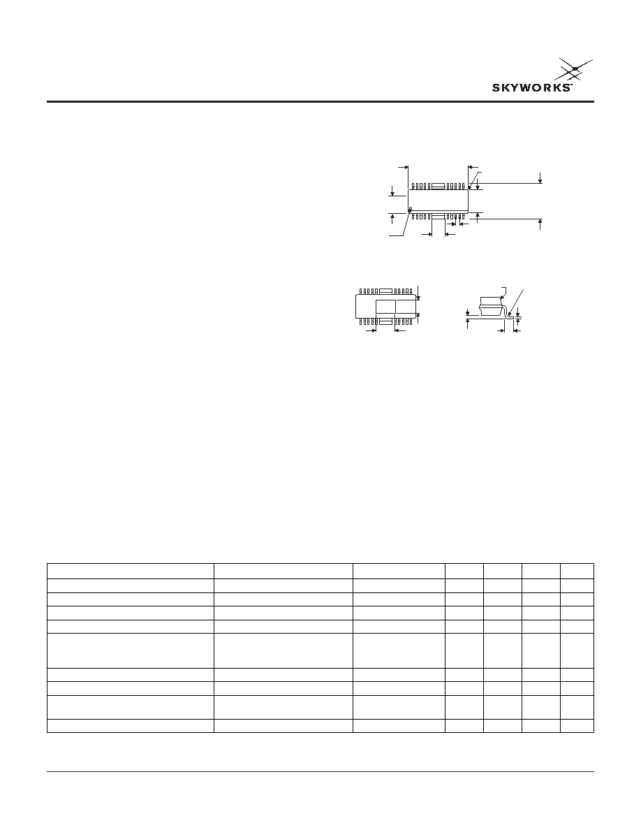
0.394 (10.00 mm)
0.386 (9.80 mm)
R 0.010
(0.25 mm) MAX.
0.157 (3.99 mm)
0.150 (3.81 mm)
0.244
(6.20 mm)
0.228
(5.79 mm)
0.087 (2.21 mm)
0.083 (2.11 mm)
0.120
(3.05 mm)
MAX.
28
15
14
0.025 BSC
0.060 (1.52 mm) REF.
0.145 (3.68 mm) REF.
0.063 (1.60 mm)
0.049 (1.24 mm)
0.050 (1.27 mm)
0.016 (0.41 mm)
0.004 MAX.
(0.010 mm)
R 0.33 (0.013 mm)
0.020 (0.008 mm)
0.38 (0.015 mm)
MAX. X 45∞
CHAMFER
PIN 1
INDICATOR
GaAs die size is reduced and the overall cost is less. This
approach also permits the flexibility to tweak the amplifier
for optimum performance at different powers, and/or
frequencies.
The board schematic demonstrates one way to present
the optimum load match while providing a path for the
DC bias.

2
Skyworks Solutions, Inc. [978] 241-7000
∑
Fax [978] 241-7906
∑
Email sales@skyworksinc.com
∑
www.skyworksinc.com
Specifications subject to change without notice. 3/99A
GaAs IC Saturated Power Amplifier 824≠849 MHz
AP104-69
30
25
20
15
10
5
0
60
50
40
30
20
10
0
-6
Input Power (dBm)
P
OUT
, P.A.E. vs. P
IN
-4
-2
0
2
4
6
8
Output Power (dBm)
Power Added Efficiency (%)
28
27
26
25
24
19
18
17
16
15
1
2
3
4
5
1
01
1
1
21
31
4
DC/DC
Converter
Bias
Control
Input Power (dBm)
Second & Third Harmonic (dBc)
0
-10
-20
-30
-40
-50
-60
-6
-4
-2
0
2
4
6
8
Third
Third
Second & Third Harmonic vs. P
IN
Second
Input Power (dBm)
Output Power (dBm)
Gain (dB)
40
35
30
25
20
15
10
5
0
40
35
30
25
20
15
10
5
0
-6
-4
-2
0
2
4
6
8
P
OUT
, Gain vs. P
IN
Input Power (dBm)
I
DD
, Supply Current (mA)
400
350
300
250
200
150
100
50
-6
-4
-2
0
2
4
6
8
I
DD
vs. P
IN
Typical Performance Data (824≠849 MHz)
Pin Out
Pin Out Assignments
Pin 1: V
REF
Reference voltage for bias control circuitry. 1.2K resistor
between this pin and Pin 28 needed to set nominal drain
currents.
Pin 2: V
GS2
Second stage gate voltage tap. Should be bypassed as
shown.
Pin 3: V
DS1
First stage drain bias feed. Requires a matching inductor
with good RF bypassing and the +4.8 V nominal supply
voltage.
Pin 4: V
GS1
First stage gate voltage tap. Requires similar RF
bypassing as Pin 2 and a 22K resistor to properly bias the
first stage.

Skyworks Solutions, Inc. [978] 241-7000
∑
Fax [978] 241-7906
∑
Email sales@skyworksinc.com
∑
www.skyworksinc.com
3
Specifications subject to change without notice. 3/99A
GaAs IC Saturated Power Amplifier 824≠849 MHz
AP104-69
Pin 5: RF In
RF input with a 33 pF series input matching capacitor.
Pin 6-14: GND
Connect to ground.
Pin 15: V
GEN
Supply voltage to DC/DC converter. Requires 3.75 V with
100 nF of bypassing.
Pin 16: V
SS OUT
Negative output voltage from DC/DC converter. Two
bypassing capacitors, a 100 nF and a 33 pF capacitor, are
required. This voltage should be supplied to the bias
controller network at Pin 27. External circuitry (LCD
display, driver amplifiers, etc.) can tap off the negative
voltage at this point. A maximum of 2 mA can be supplied.
Pin 17: CB
Switched capacitor for DC/DC converter. A 100 nF
capacitor must be connected between Pin 17 and Pin 18
with a minimal distance between the capacitor and
the chip.
Pin 18: CA
Switched capacitor for DC/DC converter, shared with
Pin 17.
Pin 19≠23: GND
Connect to ground.
Pin 24≠26: RF Out/V
DD2
RF output and bias injection for the second stage drain.
Output matching circuitry is required to transform the
optimum load impedance to 50
. The circuit must also
provide a path for the +4.8 V DC bias and have good RF
bypassing.
Pin 27: V
SS IN
Negative voltage for the bias controller circuit. The negative
voltage from the DC/DC converter, Pin 16, should be fed
to this pin.
Pin 28: V
DD
Bias controller supply voltage. The regulated +3.75 V
supply must be connected to this pin. Disconnecting this
voltage will turn the PA bias off. A switch at this pin can
turn the PA on or off while leaving V
GEN
connected and
the negative supply unchanged. A 1.2K resistor must be
connected between this pin and Pin 1.
Pin Configuration
Terminal
Symbol
Function
1
V
REF
Reference Voltage
2
V
GS2
Gate Voltage 2
3
V
DS1
Drain Supply Voltage 1
4
V
GS1
Gate Voltage 1
5
RF In
RF Input
6
GND
Ground
7
GND
Ground
8
GND
Ground
9
GND
Ground
10
GND
Ground
11
GND
Ground
12
GND
Ground
13
GND
Ground
14
V
REF
Voltage Generator Ground
15
V
GEN
Generator Voltage
16
V
SS OUT
Negative Bias Voltage Out
17
CB
Generator Flying Cap
18
CA
Generator Flying Cap
19
GND
Ground
20
GND
Ground
21
GND
Ground
22
GND
Ground
23
GND
Ground
24
RF Out/V
DS2
RF Output/Supply Voltage 2
25
RF Out/V
DS2
RF Output/Supply Voltage 2
26
RF Out/V
DS2
RF Output/Supply Voltage 2
27
V
SS IN
Negative Bias Voltage In
28
V
DD
Positive Bias Voltage

4
Skyworks Solutions, Inc. [978] 241-7000
∑
Fax [978] 241-7906
∑
Email sales@skyworksinc.com
∑
www.skyworksinc.com
Specifications subject to change without notice. 3/99A
GaAs IC Saturated Power Amplifier 824≠849 MHz
AP104-69
Bias Controller Circuit
An on-chip bias controller circuit eliminates the need to
individually adjust the gate bias voltages. This circuit uses
3.75 V and the negative voltage from the DC converter
(-2.7 V to -3.75 V) to set the gate voltages on each stage
for the proper bias current.
Standby Mode
The power amplifier should be turned off whenever
possible in order to reduce the overall power consumption.
The AP104 can be turned off in several ways. The simplest
is to switch the bias controller supply voltage (Pin 28)
open. The gate bias voltages are in turn reduced from their
nominal voltages to V
SS
, resulting in a PA bias current of
less than 1 mA. Additional PMOS switches in the drain
lines drop the bias-off currents to <10 µA.
Circuit Layout
GND
GND
GND
GND
GND
33 pF
RF In
22 K
22 pF
33 pF
33 pF
33 pF
22 nF
22 nF
27
220 pF
22 nF
Ferrite
6.8K
V
REF
V
GS2
V
DS1
RF In
V
GS1
V
DD
V
SS OUT
V
GEN
V
GEN
V
SS IN
RF Out
RF Out
CA
CB
RF Out
GND
100 nF
100 nF
100 pF
33 pF
10
33 pF
33 pF
33 pF
2.2 pF
8.2 nH
2.2 nH
27
220 pF
Ferrite
V
DS
V
DD
RF Out
5.6 pF
Characteristic
Value
Drain Voltage (V
DD
)
+10 V
Bias Voltage (V
SS
)
-6 V
Reference Voltage (V
REF
)
+6 V
Power Input (P
IN
)
+12 dBm
Operating Temperature (T
OPT
)
-30 to +100∞C
Storage Temperature (T
STG
)
-35 to +120∞C
Absolute Maximum Ratings