 | –≠–ª–µ–∫—Ç—Ä–æ–Ω–Ω—ã–π –∫–æ–º–ø–æ–Ω–µ–Ω—Ç: RM805 | –°–∫–∞—á–∞—Ç—å:  PDF PDF  ZIP ZIP |

Data Sheet
Skyworks Solutions, Inc., Proprietary
101505D
© 2000≠2002 Skyworks Solutions, Inc., All Rights Reserved.
December 6, 2002
RM805
Power Amplifier Module for Broadband
The RM805 Power Amplifier (PA) is a fully matched 28-pin surface mount module
designed for Private Mobile Radio (PMR), Wireless Local Loop (WLL), and Time
Division Multiple Access/Advanced Mobile Phone Service (TDMA/AMPS) mobile units
operating in the 806-849 MHz cellular bandwidth. Microwave Monolithic Integrated
Circuits (MMICs), comprised of Gallium Arsenide (GaAs) and CMOS, contain all active
circuitry in the module, which includes on-board bias circuitry as well as input and
interstage matching circuits. The output match is realized off-chip within the module
package to optimize efficiency and high power performance (P
3db_sat
35.8 dBm)
into a 50
load.
This device, manufactured with Skyworks' GaAs Heterojunction Bipolar Transistor
(HBT) and silicon CMOS processes, provides for all positive voltage DC supply
operation while maintaining high efficiency and good linearity. Primary bias to the
RM805 can be supplied directly from a single cell lithium-ion or other suitable battery
with a nominal output 3.5 Volts.
No external supply side switch is needed as typical "off" leakage is a few
microamperes with full primary voltage supplied from the battery.
Functional Block Diagram
VREG
(1)
VD4
(28)
VD2
(22)
VD3
(8)
RF IN
(5)
RF OUT
(15)
INPUT
MATCH
INTER
STAGE
MATCH 1
INTER
STAGE
MATCH 2
OUTPUT
MATCH
CMOS
CONTROLLER
CIRCUIT
PA 1
PA 2
OUTPUT
STAGE
GaAs HBT IC
MODULE
Distinguishing Features
∑
Low voltage positive bias supply
∑
Good linearity
∑
High efficiency
∑
Dual mode operation
∑
Large dynamic range
∑
28-pin LCC package
(10 x 13.97 x 1.7 mm)
∑
Power down control
Applications
∑
PMR (806≠825 MHz)
∑
TETRA (806≠825 MHz)
∑
TDMA (824≠849 MHz)
∑
AMPS (824-849 MHz)
∑
Wireless Local Loop

Electrical Specifications
RM805
Power Amplifier Module for Broadband
2
Skyworks Solutions, Inc., Proprietary
101505D
December 6, 2002
Electrical Specifications
The following tables list the electrical characteristics of the RM805 Power Amplifier.
Table 1
lists
the absolute maximum rating for continuous operation.
Table 2
lists the recommended operating
conditions for achieving the electrical performance listed in
Table 3
, which depicts the electrical
performance of the RM805 Power Amplifier over the recommended operating conditions.
Table 1. Absolute Maximum Ratings
(1)
Parameter
Symbol
Minimum
Nominal
Maximum
Unit
RF Input Power
(2)
Pin
--
≠8.0
11.0
dBm
Supply Voltage
Vcc
--
3.5
6.9
(3)
Volts
Regulation Voltage
Vreg
0.0
2.75
Vcc
(4)
Volts
Case Operating Temperature
Tc
≠30
+25
+110
∞C
Storage Temperature
Tstg
≠55
--
+125
∞C
NOTE(S):
(1)
No damage assuming only one parameter is set at limit at a time with all other parameters set at or below
nominal value.
(2)
Pulsed operation at 25% duty cycle.
(3)
When amplifier is biased off (Vreg = 0 V)
(4)
Voltage on Vreg pin may not exceed the applied Vcc voltage.
Table 2. Recommended Operating Conditions
Parameter
Symbol
Minimum
Nominal
Maximum
Unit
Supply Voltage
Vcc
3.0
3.5
4.4
Volts
Regulation Voltage
Vreg
2.65
2.75
2.85
Volts
Operating Frequency
Fo
806
--
849
MHz
Continuous RMS Output Power
PoRMS
29.0
31.0
dBm
Operating Temperature
To
≠30
+25
+85
∞C

RM805
Electrical Specifications
Power Amplifier Module for Broadband
101505D
Skyworks Solutions, Inc., Proprietary
3
December 6, 2002
Table 3. Electrical Specifications for TDMA/AMPS Nominal Operating Conditions
(1)
Characteristics
Condition
Symbol
Minimum
Typical
Maximum
Unit
Quiescent current
Vreg = 2.75
Iq
332
370
450
mA
Gain
Po = 29 dBm
G
p
35.5
38.0
40.0
dB
Saturated Output Power
Duty Cycle
25%
Gain Compression
3 dB
P3dB sat
35.3
35.8
--
dBm
Power Added Efficiency
Po = 29 dBm
Po = P3dB sat
PAEa
PAEd
21.0
48.0
23.0
52.0
--
--
%
%
Harmonic Levels
Second
Third
Fourth
Po
P3db sat
Po
P3db sat
Po
P3db sat
AFo2
AFo3
AFo4
--
--
--
≠10.0
≠30.0
≠30.0
--
--
--
dBm
dBm
dBm
Noise Power in RX Band
Fc + 30 MHz, BW = 18 kHz
Po
29 dBm
RxBN
--
--
≠85.0
dBm/Hz
Noise Figure
--
NF
--
8.0
--
dB
Input Voltage Standing Wave
Ratio
--
VSWR
--
1.3:1
2.0:1
--
Stability (Spurious output)
S
10.0:1
--
≠36.0
dBm
Ruggedness ≠ No damage
Po
29 dBm
Ru
15.0:1
--
--
VSWR
NOTE(S):
(1)
Vcc = +3.5 V, Vreg = +2.75 V, Freq = 815 MHz, Tc = 25 ∞C, Vreg pulsed at 25% duty cycle, unless otherwise specified.

Evaluation Board Description
RM805
Power Amplifier Module for Broadband
4
Skyworks Solutions, Inc., Proprietary
101505D
December 6, 2002
Evaluation Board Description
The evaluation board is a platform for testing and interfacing design circuitry. To accommodate the
interface testing of the RM805, the evaluation board schematic and assembly diagram are included
for preliminary analysis and design.
Figure 1
shows the basic schematic of the board for the
806 MHz to 849 MHz range and
Figure 2
illustrates the board layout.
Figure 1. Evaluation Board Schematic
Figure 2. Evaluation Board Assembly Diagram
1
2
3
4
5
6
8
16
15
17
18
19
20
21
9
10
11
12
13
14
22
28
27
26
25
24
23
7
VREG
VD4
VD2
RF_IN
VD3
RF_OUT
C2
10
µF
C3
1000pF
C1
10
µF
C5
1000pF
C4
10
µF
50 OHM
50 OHM
SCHEMATIC FOR TEST FIXTURE
NC
NC
NC
NC
NC
NC
101505_009
NC
NC
RM805
IDEN TEST FIXTURE
101505-007
GND
VD1
VD2
VD3
VD4
VREG
VCTL
GND
RM805
RM805
INPUT
C1
C2
+
+
C4
C7
+
+
C3
C5 C6
RM805
Package Dimensions and Pin Descriptions
Power Amplifier Module for Broadband
101505D
Skyworks Solutions, Inc., Proprietary
5
December 6, 2002
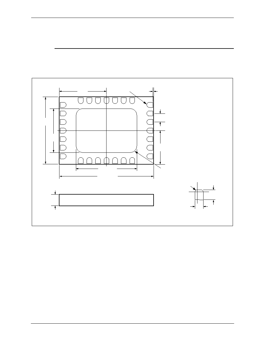
Package Dimensions and Pin Descriptions
The RM805 is a multi-layer laminate base, overmold encapsulated modular package designed for
surface mount solder attachment to a printed circuit board.
Figure 3. RM805 Package Dimensions
101505_006
6.99
BOTTOM VIEW
6.50
10.00
Exposed Center
Ground Pad
Pin 1
0.05
TYPICAL
5.00
FRONT VIEW
1.70
9.00
13.97
4 X R 0.99
28 X 0.13
0.89
0.76
R0.38
PAD
DETAIL