 | –≠–ª–µ–∫—Ç—Ä–æ–Ω–Ω—ã–π –∫–æ–º–ø–æ–Ω–µ–Ω—Ç: IrCC | –°–∫–∞—á–∞—Ç—å:  PDF PDF  ZIP ZIP |

IrCC
Infrared Communications Controller
FEATURES
∑
Multi-Protocol Serial Communications
Controller
∑
Full IrDA v1.1 Implementation: 2.4Kbps,
115.2Kbps, .576Mbps, 1.152Mbps and
4Mbps
∑
Consumer Infrared (TV Remote Control)
Interface
∑
SHARP Amplitude Shift Keyed Infrared
(ASK IR) Interface
∑
Direct Rx/Tx Infrared Diode Control (Raw)
and General Purpose Data Pins
∑
Programmable High-Speed Synchronous
Communications Engine (SCE) with a 128-
Byte FIFO and Programmable Threshold
∑
High-Speed NS16C550A-Compatible
Universal Asynchronous Receiver/
Transmitter Interface (ACE UART2) with
16-Byte Send and Receive FIFOs
∑
ISA Single-Byte and Burst-Mode DMA and
Interrupt-Driven Programmed I/O with Zero
Wait State and String Move Timing
∑
16-bit CRC-CCITT and 32-bit IEEE 802
CRC32 Hardware CRC Generators
GENERAL DESCRIPTION
This document describes the Infrared
Communications Controller (IrCC) function
which is common to a number of SMSC
products including the FDC37C669FR,
FDC37C93xFR, and FDC37C957FR devices.
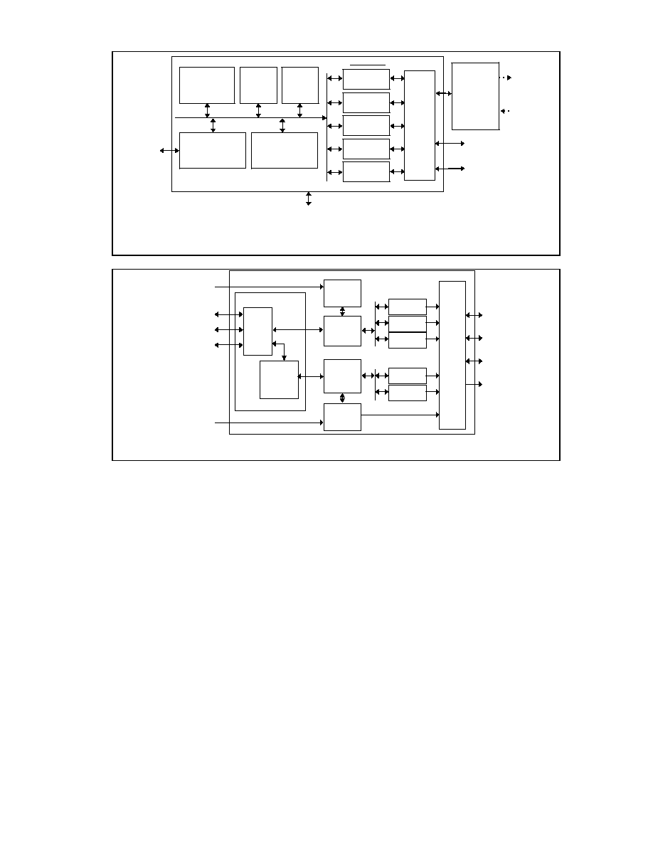
The IrCC consists of two main architectural
blocks: the ACE 16550A UART and a
Synchronous Communications Engine (SCE)
(Figure 2). Each block is supported by its own
unique register set.
The IrCC UART-driven IrDA SIR and SHARP
ASK modes are backward-compatible with early
SMSC Super I/O and Ultra I/O infrared
implementations. The IrCC SCE supports IrDA
v1.1 .576Mbps, 1.152Mbps, 4Mbps, and
Consumer IR modes. All of the SCE modes use
DMA. The IrCC offers flexible signal routing and
programmable output control through the Raw
mode interface, General Purpose Data pins and
Output Multiplexer. Chip-level address decoding
is required to access the IrCC register sets.

2
TABLE OF CONTENTS
FEATURES ...................................................................................................................................... 1
GENERAL DESCRIPTION................................................................................................................ 1
INTERFACE DESCRIPTION............................................................................................................. 4
PORTS...................................................................................................................................... 4
CHIP-LEVEL CONFIGURATION CONTROLS............................................................................ 6
RAW IR............................................................................................................................................ 8
CONSUMER IR (TV REMOTE)......................................................................................................... 9
INTRODUCTION ....................................................................................................................... 9
DESCRIPTION ........................................................................................................................ 10
IrDA SIR AND SHARP ASK IR INTERFACE ................................................................................... 14
INFRARED DATA ASSOCIATION............................................................................................ 19
REGISTERS................................................................................................................................... 24
ACE UART CONTROLS .......................................................................................................... 24
SCE CONTROLS..................................................................................................................... 25
MASTER BLOCK CONTROL REGISTER ................................................................................ 26
REGISTER BLOCK ZERO ....................................................................................................... 27
REGISTER BLOCK ONE ......................................................................................................... 32
REGISTER BLOCK TWO ........................................................................................................ 36
REGISTER BLOCK THREE ..................................................................................................... 37
REGISTER BLOCK FOUR....................................................................................................... 38
ACE UART ..................................................................................................................................... 40
REGISTER DESCRIPTION...................................................................................................... 40
SCE ............................................................................................................................................... 55
DESCRIPTION ........................................................................................................................ 55
FRAMING................................................................................................................................ 55
ACTIVE FRAME INDICATOR .................................................................................................. 55
IrDA ENCODER....................................................................................................................... 56
CONSUMER IR ENCODER ..................................................................................................... 61
LOOPBACK MODE ................................................................................................................. 63
BUS INTERFACE I/O ..................................................................................................................... 65
FIFO MULTIPLEXER ............................................................................................................... 65
128-BYTE SCE FIFO ............................................................................................................... 65
DMA ........................................................................................................................................ 67
PROGRAMMED I/O................................................................................................................. 71
IOCHRDY TIME-OUT .............................................................................................................. 73
ZERO WAIT STATE SUPPORT............................................................................................... 75
OUTPUT MULTIPLEXER................................................................................................................ 76
CHIP-LEVEL IrCC ADDRESSING SUPPORT ................................................................................. 77
AC TIMING..................................................................................................................................... 78
3
Raw
IR
IR
Transducer
Module
REGISTERS
ACE
UART
Bus Interface
I/O
Clock
Generator
COMM
Port
IrDA
IR
ASK
IR
Consumer
IR
SMC Infrared Communications Controller
Output
Mux
COM
AUX
SCE
Encoders
System
Controls
FIGURE 1 - SMSC IrCC FUNCTIONAL COMPONENTS
ACE UART
SCE
IrDA SIR
Sharp ASK
COM
IrDA FIR
Consumer
SCE
Registers
ACE
Registers
Output
MUX
FIFO,
DMA, I/O,
Interrupts
Databus
MUX
Bus Interface
nACE
ISA Controls
Data (0-7)
Address (0-2)
IR
COM
AUX
G.P.
nSCE
GP/Raw/Fast
FIGURE 2 - IrCC ARCHITECTURAL BLOCK DIAGRAM
4
INTERFACE DESCRIPTION
The Interface Description lists the signals that
are required to place the IrCC in a larger chip-
level context.
There are four groups of signals in this section:
PORT signals, HOST BUS controls, SYSTEM
controls, and CHIP-LEVEL CONFIGURATION
controls.
PORTS
The four Ports (IR, COM, AUX, and General
Purpose) provide external access for serial data
and controls. The active IrCC encoder is routed
through the Output Multiplexer to either the IR,
COM, or AUX port. The General Purpose port
provides external access for controls that are
independent of the IrCC Block Control bits or the
Output Multiplexer.
Table 1 - IR Port Signals
NAME
SIZE (BITS)
TYPE
DESCRIPTION
IRRx
1
Input
Infrared Receive Data
IRTx
1
Output
Infrared Transmit Data
Table 2 - COM Port Signals
NAME
SIZE (BITS)
TYPE
DESCRIPTION
CRx
1
Input
COM Receive Data
CTx
1
Output
COM Transmit Data
nRTS
1
Output
Request to Send
nDTR
1
Output
Data Terminal Ready
nCTS
1
Input
Clear To Send
nDSR
1
Input
Data Set Ready
nDCD
1
Input
Data Carrier Detect
nRI
1
Input
Ring Indicator
Table 3 - AUX Port Signals
(e.g., can be used for high-current drivers for Consumer IR)
NAME
SIZE (BITS)
TYPE
DESCRIPTION
ARx
1
Input
Aux. Receive Data
ATx
1
Output
Aux. Transmit Data

5
Table 4 - G. P. Port Signals
NAME
SIZE (BITS)
TYPE
DESCRIPTION
Fast
1
Output
General Purpose Data
GP Data
1
Output
General Purpose Data
Fast
The Fast pin always reflects the state of Fast, bit
6 of SCE Line Control Register A. The state of
Fast is independent of the IrCC Block Controls
or the Output Multiplexer. The Fast pin can be
used at the chip level for IR Transceiver
configuration.
GP Data
The G.P. Data pin always reflects the state of
General Purpose Data, bit 5 of SCE Line Control
Register A. The state of G.P. Data is
independent of the IrCC Block Controls or the
Output Multiplexer.
Table 5 - HOST Signals
NAME
SIZE (BITS)
TYPE
DESCRIPTION
D0-D7
8
Bidirectional
Host Data Bus
A0-A2
3
Input
IrCC Register Address Bus
nIOR
1
Input
ISA I/O Read
nIOW
1
Input
ISA I/O Write
AEN
1
Input
ISA Address Enable
DRQ
1
Output
DMA Request
nDACK
1
Input
ISA DMA Acknowledge
TC
1
Input
ISA DMA Terminal Count
IRQ
1
Output
Interrupt Request
IOCHRDY
1
Output
ISA I/O Channel Ready
nSRDY
1
Output
ISA Synchronous Ready (Zero Wait State)

6
Table 6 - SYSTEM Signals
NAME
SIZE (BITS)
TYPE
DESCRIPTION
CLK
1
Input
System Clock
RESET
1
Input
IrCC System Reset
Power Down
1
Input
Low Power Control
DMAEN
1
Output
DRQ Tristate Control
IRQEN
1
Output
IRQ Tristate Control
nACE
1
Input
ACE 550 Register Bank Select
nSCE
1
Input
SCE Register Bank Select
VCC
Power
System Supply
GND
Power
System Ground
DMAEN
DMAEN is used by the chip-level interface to
tristate the IrCC DRQ output when the DMA
Enable bit is inactive. The DMA Enable bit is
located in SCE Configuration Register B, bit 0.
IRQEN
IRQEN is used by the chip-level interface to
tristate the IrCC IRQ output when the OUT2 bit
is inactive. The OUT2 bit is located in 16550A
MODEM Control Register.
Power Down
The Power Down pin is used by the chip-level
interface to put the SCE into low power mode.
NOTE: Power Down does not force the ACE550
into low power mode.
CHIP-LEVEL CONFIGURATION CONTROLS
The following signals come from chip-level
configuration registers. There are two types of
Chip-Level Configuration Controls: IrCC-Specific
controls, and Legacy Controls. Both types have
equivalent controls in either the IrCC ACE or
SCE Registers.
The IrCC-Specific controls have been newly
added primarily to support the IrCC block.
Provisions have been made in new chip-level
configuraton contexts to accommodate these
signals.
The Legacy controls already exist in other
contexts. Provisions have been made in legacy
devices to accommodate these controls from
either the Chip-Level Configuration Registers or
the IrCC Registers; i.e., the last updated value
from either source determines the current
control state and is visible in both registers.
7
Table 7 - IRCC-Specific Chip-Level Controls
NAME
SIZE (BITS)
TYPE
DESCRIPTION
DMA Channel
4
Input
ISA DMA Channel Number
IRQ Level
4
Input
ISA Interrupt Level
DMA Channel
4-bit bus from a chip-level configuration register,
used to identify the current IrCC DMA channel
number. The value appears in the upper nibble
of IrCC Register Block Three, Address Four.
IRQ Level
4-bit bus from a chip-level configuration register,
used to identify the current IrCC IRQ level. The
value appears in the lower nibble of IrCC
Register Block Three, Address Four.
Table 8 - Legacy Chip-Level Controls
NAME
SIZE (BITS)
TYPE
DESCRIPTION
Tx Polarity
1
Input
Output Mux. Transmit Polarity
Rx Polarity
1
Input
Output Mux. Receive Polarity
Half Duplex
1
Input
16550A UART Half Duplex Control
IR Mode
3
Input
IR Mode Register Bits
IR Location
2
Input
IR Option Register Location Bits
Tx Polarity
Typically part of a 16550A Serial Port Option
Register. The value also appears in IrCC
Register Block One, Address Zero.
Rx Polarity
Typically part of a 16550A Serial Port Option
Register. The value also appears in IrCC
Register Block One, Address Zero.
Half Duplex
Typically part of a 16550A Serial Port Option
Register. The value also appears in IrCC
Register Block One, Address Zero.
IR Mode
Typically part of a 16550A Serial Port Option
Register. These values are also part of the IrCC
Block Control bits 3-5, Register Block One,
Address Zero.
IR Location
Typically part of a 16550A Serial Port IR Option
Register. These values are the IrCC Output
Mux bits, Register Block One, Address One.
NOTE: These legacy controls are uniformly
updated in the IrCC and the Top-level Device
Configuration Registers only when either set of
registers are explicitly written using IOW or
following a device-level POR. IrCC software
resets will not affect the legacy bits.

8
OPERATION MODES
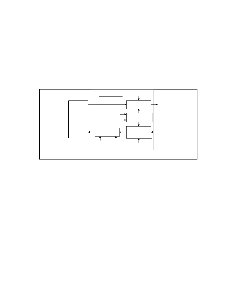
RAW IR
In Raw mode the state of the IR emitter and
detector can be directly accessed through the
host interface (Figure 3).
The IR emitter tracks the Raw Tx Control bit.
For example, depending on the state of the Tx
Polarity control a logic '1' may turn the LED on
and a logic '0' may turn the LED off. Care must
be taken in software to ensure that the LED is
not on continuously.
The Raw Rx Control bit represents the state of
the PIN diode. For example, depending on the
state of the Rx Polarity control a logic '1' may
mean no IR is detected, a logic '0' may mean IR
is being detected. If an IR carrier is being
received, the Raw Rx Control bit will oscillate at
the carrier frequency.
If enabled, a Raw Mode Interrupt will be
generated when the Raw Rx Control bit
transitions to the active state, depending on the
state of the Rx Polarity control.
RAW Tx
Registers
Transition
Detect
Enable
Interrupt
Encoder/Decoder
RAW Rx
FIGURE 3 - RAW IR BLOCK DIAGRAM
9
CONSUMER IR (TV REMOTE)
INTRODUCTION
The IrCC Consumer IR (TV Remote) block is a
general-purpose programmable Amplitude Shift
Keyed serial communications interface that
includes a Carrier Frequency Divider, a
Programmable Receive Carrier Range
Sensitivity Register, and Receive and Transmit
Modulators (Figure 4).
The Consumer IR block transfers data between
the SCE and Output Multiplexer without framing
as a fixed bit-cell serial NRZ data stream. The
components of this block can also modulate and
demodulate serial data at programmable bit
rates and carrier frequencies.
Variable length encoding and all packet framing
is handled by system software. Consequently,
many encoding methods, modulation
frequencies and bit rates can be supported,
including 38KHz PPM, PWM and RC-5 TV
Remote formats.
Register controls for this block can be found in
Register Block Two. They are the Consumer IR
Control Register, the Consumer IR Carrier Rate
Register, and the Consumer IR Bit Rate
Register.
SCE
Transmit Bit-Rate
Divider
Carrier Frequency
Divider
Clock
Programmable
Receive Carrier
Sense
Receive Bit-Rate
Divider
TV Tx
Tx Enable
Range
Sync
Rx Enable
Encoder/Decoder
Carrier Off
TV Rx
FIGURE 4 - IRCC CONSUMER IR (TV REMOTE) BLOCK

10
DESCRIPTION
Carrier Frequency Divider
The Carrier Frequency Divider register is used
to program the ASK carrier frequency for the
transmit modulator and receive detector (Figure
5). The divider is eight bits wide.
The input clock to the Carrier Frequency Divider
is 1.6MHz (48MHz
˜
30). The relationship
between the divider value (CFD) and the carrier
frequency (Fc) is as follows:
CFD = (1.6MHz/Fc) - 1
For example, program the Carrier Frequency
Divider register with 41 ('29'Hex) for a 38KHz TV
Remote: Fc = 38.095KHz. This is ~.25%
accuracy. Table 9 contains representative CFD
vs. Carrier Frequency relationships.
The Carrier Frequency range is 1.6MHz to
6.25KHz.
The carrier frequency encoder/decoder can be
defeated using the Carrier Off bit. When Carrier
Off is one, the transmitter outputs a non-
modulated SCE serial NRZ data stream at the
programmed bit rate; the receiver does not
attempt to demodulate a carrier from the
incoming serial data stream.
Table 9 - Representative Carrier Frequencies
CFD
Fc (KHz)
CFD
Fc (KHz)
CFD
Fc (KHz)
CFD
Fc (KHz)
001
800.000
065
24.242
129
12.308
193
8.247
005
266.667
069
22.857
133
11.940
197
8.081
009
160.000
073
21.622
137
11.594
201
7.921
013
114.286
077
20.513
141
11.268
205
7.767
017
88.889
081
19.512
145
10.959
209
7.619
021
72.727
085
18.605
149
10.667
213
7.477
025
61.538
089
17.778
153
10.390
217
7.339
029
53.333
093
17.021
157
10.127
221
7.207
033
47.059
097
16.327
161
9.877
225
7.080
037
42.105
101
15.686
165
9.639
229
6.957
041
38.095
105
15.094
169
9.412
233
6.838
045
34.783
109
14.545
173
9.195
237
6.723
049
32.000
113
14.035
177
8.989
241
6.612
053
29.630
117
13.559
181
8.791
245
6.504
057
27.586
121
13.115
185
8.602
249
6.400
061
25.806
125
12.698
189
8.421
253
6.299

11
Bit Rate Divider
The Transmit and Receive Bit Rate Divider
register is used to extract a serial NRZ data
stream for the IrCC SCE. The divider is eight
bits wide.
The input clock to the Bit Rate Divider is
100KHz (Carrier Frequency Divider input clock
˜
16). The relationship between the Bit Rate
Divider (BRD) and the Bit Rate (Fb) is as
follows:
BRD = (.1MHz/Fb) - 1
For example, program the Bit Rate Divider with
55 ('37'Hex) for a .562ms TV Remote bit cell:
Fb = 1.786KHz. This is ~.5% accuracy. Table
10 contains representative BRD vs. Bit Rate
relationships. The Bit Rate range is 100KHz to
390.625Hz.
Table 10 - Representative Bit Rates
BRD
Fb (KHz)
BRD
Fb (KHz)
BRD
Fb (KHz)
BRD
Fb (KHz)
003
25.000
067
1.471
131
0.758
195
0.510
007
12.500
071
1.389
135
0.735
199
0.500
011
8.333
075
1.316
139
0.714
203
0.490
015
6.250
079
1.250
143
0.694
207
0.481
019
5.000
083
1.190
147
0.676
211
0.472
023
4.167
087
1.136
151
0.658
215
0.463
027
3.571
091
1.087
155
0.641
219
0.455
031
3.125
095
1.042
159
0.625
223
0.446
035
2.778
099
1.000
163
0.610
227
0.439
039
2.500
103
0.962
167
0.595
231
0.431
043
2.273
107
0.926
171
0.581
235
0.424
047
2.083
111
0.893
175
0.568
239
0.417
051
1.923
115
0.862
179
0.556
243
0.410
055
1.786
119
0.833
183
0.543
247
0.403
059
1.667
123
0.806
187
0.532
251
0.397
063
1.563
127
0.781
191
0.521
255
0.391

12
Receive Carrier Sense
The Programmable Receive Carrier Sense
register is used to program the Consumer IR
decoder to detect the presence of IR energy in
a wide-to-narrow range of carrier frequencies.
The register is two bits wide.
The range values are shown in Table 11.
Carriers that fall outside of the Receive Carrier
range sensitivity "abort" the message; i.e., the
Abort bit is set, an EOM Interrupt is generated,
and the receiver is disabled. If the "Carrier Off"
bit is active, the Receive Carrier range
sensitivity is disabled.
Table 11 - Receive Carrier Sense Range
D1
D0
RANGE
0
0
±
10%
0
1
±
20%
1
0
±
40%
1
1
reserved
1
0
1
SCE Tx Data
TV Tx Output
Transmitter
TV Rx Input
SCE Rx Data
Driver
Receiver
1/Carrier
1/Bit Rate
No Light
Light
Light
No Light
Tx Polarity bit = 1
(default)
R x P o larity bit = 0
(default)
FIGURE 5 - TV REMOTE ASK ENCODE/DECODE
13
Receiver Bit Cell Synchronization
The Consumer IR Receiver demodulates
incoming ASK waveforms into NRZ data for the
SCE. The IrCC uses the edges of the
demodulated incoming infrared data to indicate
changes in bit state.
For continuous periods of high or low data
without transitions, the IrCC samples the signal
level in the center of each incoming bit period.
Using the Receiver Bit Cell Synchronization
mechanism, any transition resets the timer that
is used in the sampling process to eliminate
errors due to timing differences between the
receive decoder and the incoming bit period
(Figure 6).
Receiver synchronization can be disabled to
allow direct sampling of the demodulated
incoming infrared data stream at some preset
receive bit rate. This is useful in situations
where the speed of the receive data is not
strictly known. In such cases, the receive bit
rate is set as high as possible, the Receiver Bit
Cell Synchronization is disabled, and the system
software is used to measure the bit-cell period
from the oversampled data. The learned
parameters can then be used to switch to the
synchronized, fixed bit-cell mode to reduce
processing overhead in the host CPU for all
future transactions.
1
1
0
0
0
0
1
1
1
Sync
Sync
1
1
0
0
0
1
1
1
1
IR Rx Data
IR Rx Data
NRZ Rx Data
(SYNC)
NRZ Rx Data
(No SYNC)
1
2
3
4
5
6
7
8
9
10
Clock
1
2
3
4
5
6
7
8
9
10
11
Clock
0
FIGURE 6 - TV REMOTE RECEIVER: SYNC VS. NO SYNC

14
IrDA SIR AND SHARP ASK IR INTERFACE
This infrared interface provides a two-way
wireless communications port using infrared as
a transmission medium. Two infrared
implementations have been provided in this
block of the IrCC, IrDA SIR and Sharp ASK IR.
IrDA SIR allows serial communication at baud
rates up to 115K Baud. Each word is sent
serially beginning with a zero value start bit. A
zero is signaled by sending a single infrared
pulse at the beginning of the serial bit time. A
one is signaled by sending no infrared pulse
during the bit time. Please refer to Figure 7-
Figure 10 for the parameters of these pulses
and the IrDA waveform.
The ASK infrared allows serial communication
at baud rates up to 19.2K Baud. Each word is
sent serially beginning with a zero value start
bit. A zero is signaled by sending a 500KHz
waveform for the duration of the serial bit time.
A one is signaled by sending no transmission
during the bit time. Please refer to the AC
timing for the parameters of the ASKIR
waveform.
If the Half Duplex option is chosen, there is a
time-out when the direction of the transmission
is changed. This time-out starts at the last bit
transferred during a transmission and blocks the
receiver input until the time-out expires. If the
transmit buffer is loaded with more data before
the time-out expires, the timer is restarted after
the new byte is transmitted. If data is loaded
into the transmit buffer while a character is
being received, the transmission will not start
until the time-out expires after the last receive
bit has been received. If the start bit of another
character is received during this time-out, the
timer is restarted after the new character is
received. The time-out is programmable up to a
maximum of 10ms through the IR Half-Duplex
Time-Out Configuration Register.

15
PARAMETER
MIN
TYP
MAX
UNITS
t1
Pulse Width at 115kbaud
1.4
1.6
2.71
µ
s
t1
Pulse Width at 57.6kbaud
1.4
3.22
3.69
µ
s
t1
Pulse Width at 38.4kbaud
1.4
4.8
5.53
µ
s
t1
Pulse Width at 19.2kbaud
1.4
9.7
11.07
µ
s
t1
Pulse Width at 9.6kbaud
1.4
19.5
22.13
µ
s
t1
Pulse Width at 4.8kbaud
1.4
39
44.27
µ
s
t1
Pulse Width at 2.4kbaud
1.4
78
88.5
µ
s
t2
Bit Time at 115kbaud
8.68
µ
s
t2
Bit Time at 57.6kbaud
17.4
µ
s
t2
Bit Time at 38.4kbaud
26
µ
s
t2
Bit Time at 19.2kbaud
52
µ
s
t2
Bit Time at 9.6kbaud
104
µ
s
t2
Bit Time at 4.8kbaud
208
µ
s
t2
Bit Time at 2.4kbaud
416
µ
s
NOTES:
1. IrDA @ 115k is HPSIR compatible. IrDA @ 2400 will allow compatibility with HP95LX and 48SX.
2. IRRX: CRC Bit 1: 1 = XMIT active low
nIRRX: CRC Bit 1: 0 = XMIT active high (default)
t1
t2
t2
t1
0
1
0
1
0
0
1
1
0
1
1
DATA
IRRX
nIRRX
FIGURE 7 - IrDA RECEIVE TIMING
16
PARAMETER
MIN
TYP
MAX
UNITS
t1
Pulse Width at 115kbaud
1.41
1.6
2.71
µ
s
t1
Pulse Width at 57.6kbaud
1.41
3.22
3.69
µ
s
t1
Pulse Width at 38.4kbaud
1.41
4.8
5.53
µ
s
t1
Pulse Width at 19.2kbaud
1.41
9.7
11.07
µ
s
t1
Pulse Width at 9.6kbaud
1.41
19.5
22.13
µ
s
t1
Pulse Width at 4.8kbaud
1.41
39
44.27
µ
s
t1
Pulse Width at 2.4kbaud
1.41
78
88.55
µ
s
t2
Bit Time at 115kbaud
8.68
µ
s
t2
Bit Time at 57.6kbaud
17.4
µ
s
t2
Bit Time at 38.4kbaud
26
µ
s
t2
Bit Time at 19.2kbaud
52
µ
s
t2
Bit Time at 9.6kbaud
104
µ
s
t2
Bit Time at 4.8kbaud
208
µ
s
t2
Bit Time at 2.4kbaud
416
µ
s
NOTES:
1. Receive Pulse Detection Criteria: A received pulse is conidered detected if the received pulse is a
minimum of 1.41
µ
s
2. IRTX: CRC Bit 0: 1 = RCV active low
nIRTX: CRC Bit 0: 0 = RCV active high (default)
t1
t2
t2
t1
0
1
0
1
0
0
1
1
0
1
1
DATA
IRTX
nIRTX
FIGURE 8 - IrDA TRANSMIT TIMING
17
PARAMETER
MIN
TYP
MAX
UNITS
t1
Modulated Output Bit Time
µ
s
t2
Off Bit Time
µ
s
t3
Modulated Output "On"
0.8
1
1.2
µ
s
t4
Modulated Output "Off"
0.8
1
1.2
µ
s
t5
Modulated Output "On"
0.8
1
1.2
µ
s
t6
Modulated Output "Off"
0.8
1
1.2
µ
s
NOTES:
1. IRTX: CRC Bit 1: 1 = XMIT active low
nIRTX: CRC Bit 1: 0 = XMIT active high (default)
MIRTX, nMIRTX are the modulated outputs.
t1
t2
t3
t4
t5
t6
0
1
0
1
0
0
1
1
0
1
1
DATA
IRTX
nIRTX
MIRTX
nMIRTX
FIGURE 9 - AMPLITUDE SHIFT KEYED IR TRANSMIT TIMING

18
PARAMETER
MIN
TYP
MAX
UNITS
t1
Modulated Output Bit Time
µ
s
t2
Off Bit Time
µ
s
t3
Modulated Output "On"
0.8
1
1.2
µ
s
t4
Modulated Output "Off"
0.8
1
1.2
µ
s
t5
Modulated Output "On"
0.8
1
1.2
µ
s
t6
Modulated Output "Off"
0.8
1
1.2
µ
s
NOTES:
1. IRRX: CRC Bit 1: 1 = RCV active low
nIRRX: CRC Bit 1: 0 = RCV active high (default)
MIRRX, nMIRRX are the modulated outputs.
t1
t2
t3
t4
t5
t6
0
1
0
1
0
0
1
1
0
1
1
DATA
IRTX
nIRTX
MIRTX
nMIRTX
FIGURE 10 - AMPLITUDE SHIFT KEYED IR RECEIVE TIMING
19
INFRARED DATA ASSOCIATION
Description
The Infrared Data Association (IrDA) was
created to develop an interoperable, low-cost,
low-power, half-duplex serial data
interconnection standard that supports a walk-
up, point-to-point user model that is adaptable
to a wide range of appliances and devices.
The IrDA Serial Infrared Data Link Standard,
Version 1.1 is the standard to which the SMSC
IrCC conforms. Relevant IrDA documents in
this specification include the SIR-Physical Layer
Specification, Version 1.1, October 17, 1995,
the SIR-Link Access Protocol (IrLAP), Version
1.0, June 23, 1994, and the Link Management
Protocol (IrLMP), Version 1.1, January 23,
1996.
The high-speed extensions (FIR) to the IrDA
physical layer as described in the SIR-Physical
Layer Specification appear as alternate
modulation and demodulation paths for data
from IrLAP bound for the IR medium and are
transparent to IrLAP as it is defined for SIR.
IR hardware and software must comply as a
system with the entire family of IrDA
specifications, including the SIR/FIR-Physical
Layer Specifications, IrLAP, and IrLMP.
A block diagram of one end of an IrDA link that
includes the SIR and FIR physical
implementations is shown in Figure 11.
SIR Interaction Pulse
The SIR Interaction Pulse (SIP) is intended to
guarantee non-disruptive coexistence with SIR-
only systems which might otherwise interfere
with Fast IR links.
A SIP is defined as a 1.6 microsecond
transmitter on pulse followed by 7.1
microseconds of off time (Figure 12). Once a
Fast connection has been established the
station must generate one SIP every 500ms.
1.152Mb/s
4Mb/s
SIR Encoder
SCE
IR
Transceiver
Module
IR Out
IR In
FIR Encoders
UART
SIP
FIGURE 11 - IRCC IRDA BLOCK DIAGRAM

20
The SIR Interaction Pulse is controlled by the
IrCC configuration register SIP ENABLE bit and
a timer. The IrCC transmits an SIR Interaction
Pulse every 500ms when the SIP enable is
active, an IrDA FIR mode has been selected,
and the transmitter or receiver is not otherwise
engaged.
The timer that controls the SIP pulse is reset
whenever 1) the SIP enable is inactive, 2) an
active FIR frame is being transmitted or
received or, 3) during an active SIP pulse. The
timer is decrementing whenever the SIP enable
bit is active and the SIP pulse generator, the
transmitter, and the receiver are inactive. When
the timer reaches zero, the SIP pulse generator
is activated (Figure 13).
1.6us
8.7us
SIP
Active SIP
Time
FIGURE 12 - SIR INTERACTION PULSE
Active Frame
SIP Enable
Reset SIP
Timer
SIP Timer
Countdown
Active SIP
Time
SIP Timer
Zero
FIGURE 13 - SIP CONTROL TIMING
21
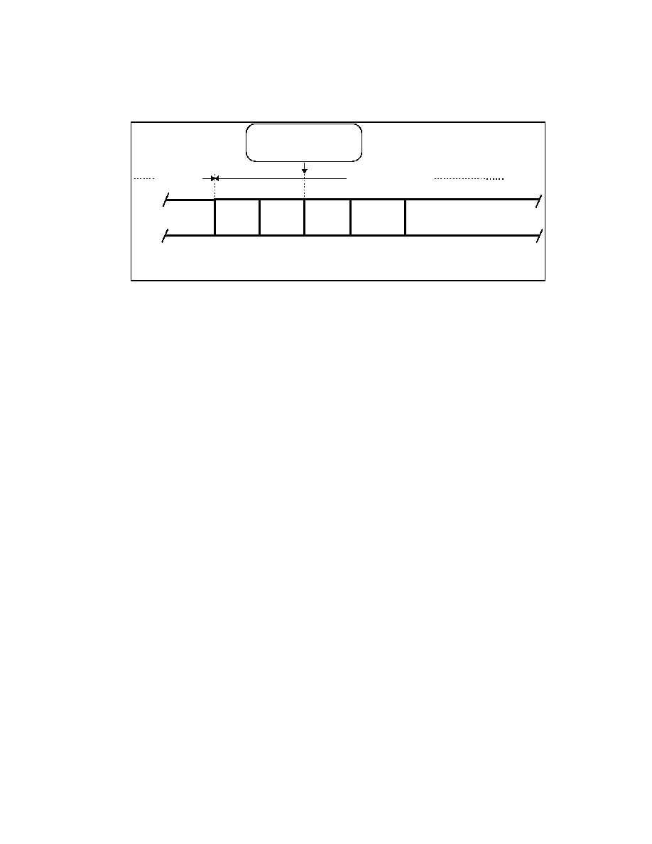
HDLC BOF Counting
The IrCC can account for system-dependent
limitations such as long interrupt latencies and
transceiver stabilization times by increasing the
number of STA flags at the beginning of every
HDLC frame (Figure 14).
The BOF COUNT register contains the number
additional start flags that are to be appended to
the standard BOF characters.
NOTE: the BOF COUNT extensions only apply
to messages that start from an idle line state;
i.e., BOF counting does not apply to brick walled
messages.
HDLC Back-to-Back Frame Transmission
HDLC back-to-back, or brick walled frames are
allowed with two or more flags, '7E'hex, in
between. If two consecutive frames are not
back-to-back, the gap between the last STO flag
of the first frame and the first STA field of the
second frame are separated by at least seven
bit times (abort sequence).
The IrDA FIR 1.152Mbps and .576Mbps
physical layer specification allows back-to-back
message packets with three flag characters
which act as the closing flag of the first frame
and the opening flags of the brick walled packet.
Additional flags can be added by programming
the Brick Wall Count register (Figure 15).
NOTE: The BOF COUNT extensions do not
apply to brick walled messages.
ADDR
8-bit Address
Field
STA
'01111110'
binary
DATA
8-bit Control field plus up to 2K - 3 bytes
Information Field
STA
'01111110'
binary
BOF COUNT register
Appends 0 - 4095 Flags to
Beginning of Frame
FIGURE 14 - EXTENDED BEGINNING-OF-FRAME

22
4PPM BOF Counting
The IrCC can account for system-dependent
limitations such as long interrupt latencies and
transceiver stabilization times by increasing the
number of PA flags at the beginning of every
4PPM frame (Figure 16).
The BOF COUNT register contains the number
of additional PA bytes that are to be appended
to the standard 4PPM BOF characters.
NOTE: The BOF COUNT extensions only apply
to messages that start from an idle line state;
i.e., BOF counting does not apply to brick walled
messages.
ADDR
8-bit Address
Field
STO
'01111110'
binary
FCS
CCITT 16-bit
CRC
DATA
8-bit Control field plus up to 2K - 3 bytes
Information Field
Brick Walled Frame
Previous
Frame
STA
'01111110'
binary
BW COUNT register
Inserts 0 - 4095 Flags between
Brick Walled Frames
STA
'01111110'
binary
FIGURE 15 - BRICK WALLED HDLC FRAMES
ADDR
8-bit Address
Field
DATA
8-bit Control field plus up to 2K - 3 bytes
Information Field
BOF COUNT register
Appends 0 - 4095 PA Bytes
to Beginning of Frame
...
PA (#16)
PA (#1)
STA
8-bit Start
Field
FIGURE 16 - 4PPM EXTENDED BOF
23
4PPM Back-to-Back Frame Transmission
Back-to-back, or brick walled frames are
allowed with 32 or more PA flag bytes between
the STO field of the first frame and the STA field
of the second frame.
Additional flags can be added by programming
the Brick Wall Count register.
NOTE: the BOF COUNT extensions do not
apply to brick walled messages.
ADDR
8-bit Address
Field
16-byte
PA
Sequence
DATA
8-bit Control field plus up to
2K - 3 bytes Information Field
Brick Walled Frame
Previous
Frame
STA
BW COUNT register
Inserts 0 - 4095 PA Bytes
between Brick Walled
Frames
STO
16-byte
PA
Sequence
FIGURE 17 - BRICK WALLED 4MBPS FRAMES

24
REGISTERS
The IrCC is partially enabled through binary
controls found in two 8-byte register banks. The
banks, the ACE550 UART Controls and the SCE
Controls, are selected with the nACE and nSCE
register-bank selector inputs found in the
Interface Description.
If nACE is zero, the three least significant bits of
the Host Address Bus decode the 16550A UART
control registers. If nSCE is zero, the SCE
control bank is addressed. All of the IrCC
registers are 8 bits wide.
ACE UART CONTROLS
The table below (Table 12) lists the ACE UART
Control Registers (see the ACE UART section).
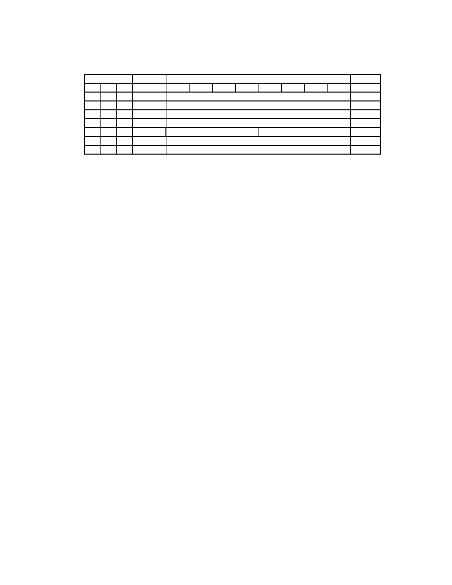
Table 12 - 16550A UART Addressing
DLAB
A2
A1
A0
DIRECTION
REGISTER NAME
0
0
0
0
Read
Receive Buffer
0
0
0
0
Write
Transmit Buffer
0
0
0
1
Read/Write
Interrupt Enable
X
0
1
0
Read
Interrupt Identification
X
0
1
0
Write
FIFO Control
X
0
1
1
Read/Write
Line Control
X
1
0
0
Read/Write
Modem Control
X
1
0
1
Read/Write
Line Status
X
1
1
0
Read/Write
Modem Status
X
1
1
1
Read/Write
Scratchpad
1
0
0
0
Read/Write
Divisor (LSB)
1
0
0
1
Read/Write
Divisor (MSB)

25
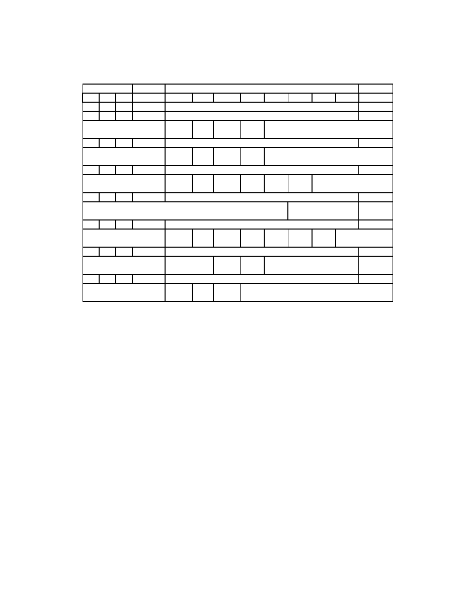
SCE CONTROLS
The IrCC SCE Registers are arranged in 7-byte
blocks. Of the eight possible register blocks,
five are used in this implementation.
The Master Block Control Register controls
access to the register blocks.
Table 13 lists all of the SCE registers in all
blocks.
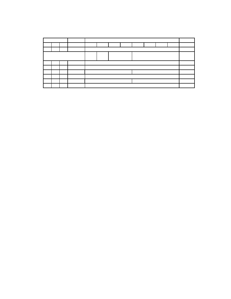
Table 13 - SCE Register Addressing
BLOCK
ADDRESS
DIRECTION
REGISTER NAME
X
7
R/W
Master Control
0
0
R/W
Data Register
0
1
RO
Interrupt Identification
0
2
R/W
Interrupt Enable
0
3
RO
Line Status (read)
0
3
WO
Line Status Address (write)
0
4
R/W
Line Control A
0
5
R/W
Line Control B
0
6
R/W
Bus Status
1
0
R/W
SCE Configuration A
1
1
R/W
SCE Configuration B
1
2
R/W
FIFO Threshold
2
0
R/W
Consumer IR Control
2
1
R/W
Consumer IR Carrier Rate
2
2
R/W
Consumer IR Bit Rate
3
0
RO
SMSC ID (high)
3
1
RO
SMSC ID (low)
3
2
RO
CHIP ID
3
3
RO
VERSION Number
3
4
RO
IRQ Level
DMA Channel
4
0
R/W
IrDA Control
BOF Count (high)
4
1
R/W
BOF Count (low)
4
2
R/W
Brick Wall Count (low)
4
3
R/W
BW Count (high)
Tx Data Size (high)
4
4
R/W
Tx Data Size (low)
4
5
R/W
Rx Data Size (high)
4
6
R/W
Rx Data Size (low)

26
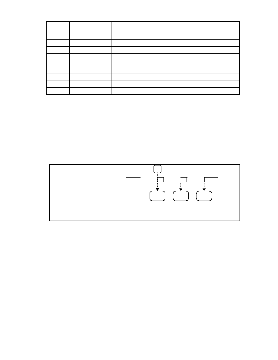
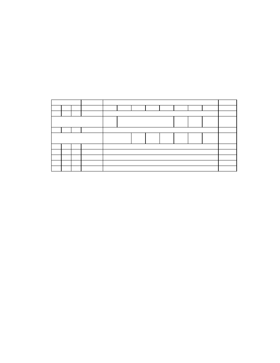
MASTER BLOCK CONTROL REGISTER
The Master Block Control Register contains the
IrCC Power Down bit, two reset bits, the Master
Interrupt Enable bit, and the Register Block
Select lines (Table 14).
Address seven is solely reserved for the Master
Block Control register. If the nSCE input is
zero, the MBC is always visible, regardless of
the state of the Register Block Select lines.
Table 14 - SCE Master Block Control Register
Address
Direction
Description
Default
A2
A1
A0
D7
D6
D5
D4
D3
D2
D1
D0
1
1
1
R/W
Master Block Control Register
'00'hex
power
down
master
reset
master
int en.
error
reset
register block
select
Register Block Select, bits 0-2
The Register Block Select bits enable access to
each of the eight possible register blocks. To
access a register block other than the default
(0), write a 3-bit register block number to the
least significant bits of the Master Block Control
Register. All subsequent reads and writes to
addresses 0 through 6 will access the registers
in the new block. To return to register block 0,
rewrite zeros to the register block select bits.
Error Reset, bit 4
Writing a one to the Error Reset bit will return all
of the SCE Line Status Register bits (Register
Block Zero) to their inactive states and reset the
Message Count bits to zero.
Master Interrupt Enable, bit 5
Setting the Master Interrupt Enable to a one
enables all of the SCE interrupts only if their
individual controls are enabled. Setting this bit
to a zero disables all SCE interrupts regardless
of the state of their individual enables.
Master Reset, bit 6
Setting the Master Reset bit to a one forces data
in the SCE registers and SCE logical blocks into
the Power-On-Reset state. The Master Reset
bit is reset to zero following the reset operation.
NOTE: The Legacy bits (Register Block One,
Address Zero, Bits D0-D6) are unaffected by
Master Reset.
Power Down, bit 7
Setting this bit to a one causes only the SCE to
enter the low-power state. Power down mode
does not preclude access to the Master Block
Control register so that this mode can be
maintained entirely under software control.
27
REGISTER BLOCK ZERO
Register Block Zero contains the SCE Data
Register, the Interrupt Control/Status registers,
the Line Control/Status registers, and the Bus
Status register (Table 15).
Typically, the controls in Register Block Zero are
used during IrDA FIR and Consumer IR
message transactions.
Table 15 - Register Block Zero
Address
Directio
n
Description
Default
A2
A1
A0
D7
D6
D5
D4
D3
D2
D1
D0
0
0
0
R/W
Data Register
0
0
1
RO
Interrupt Identification Register
'00'hex
active
frame
eom
raw
mode
fifo
0
1
0
R/W
Interrupt Enable Register
'00'hex
active
frame
eom
raw
mode
fifo
0
1
1
RO
Line Status Register (read)
'00'hex
under-
run
over-
run
frame
error
size
error
crc
error
frame
abort
0
1
1
WO
Line Status Address Register (write)
status register
address
1
0
0
R/W
Line Control Register A
'00'hex
fifo
reset
fast
g. p.
data
raw
tx
raw
rx
abort
data
done
1
0
1
R/W
Line Control Register B
'00'hex
sce modes
bits
sip
enable
brick
wall
message
count
1
1
0
RO
Bus Status Register
'00'hex
not
empty
fifo
full
time-
out
Data Register (Address 0)
The Data Register is the FIFO access port.
Typically, the user will only write to the FIFO
when transmitting and read from the FIFO when
receiving. The Host always has read access to
the FIFO regardless of the state of the SCE
Modes bits or the Loopback bit. Host read
access to the FIFO is blocked when the FIFO is
empty. The Host has write access to the FIFO
only when the Loopback bit is inactive and the
SCE Modes bits are zero or Transmit mode
Is enabled. Host write access to the FIFO is
blocked when the FIFO is full.
Interrupt Identification Register (Address 1)
Active Frame, bit 7
When this bit is one, an Active Frame has
occurred (see the Active Frame Indicator
section). The Active Frame typically indicates
that the SCE receiver has detected a valid
incoming IrDA FIR or TV Remote start-of-frame
sequence. Reading the Interrupt Identification
register resets the Active Frame bit.

28
EOM, bit 6
When this bit is one, an End of Message has
occurred. The EOM indicates the end of an
IrDA FIR EOF or Abort. During Consumer IR
messages EOM also indicates FIFO underruns/
overruns and DMA Terminal Counts. Reading
the Interrupt Identification register resets the
EOM bit.
Raw Mode Interrupt, bit 5
When this bit is one, a Raw Mode interrupt has
occurred. The Raw Mode Interrupt indicates
that the Raw Rx Control bit has gone active.
Reading the Interrupt Identification register
resets the Raw Mode Interrupt bit.
FIFO Interrupt, bit 4
When this bit is one, a FIFO Interrupt has
occurred. The FIFO Interrupt indicates that the
FIFO Interrupt Enable is active and either a
TxServReq or an RxServReq has occurred. The
FIFO Interrupt bit is cleared when the interrupt is
disabled; i.e., reading the Interrupt Identification
register does not reset the FIFO Interrupt bit.
Interrupt Enable Register (Address 2)
Setting any of the bits in this register to one
enables the associated interrupt (see the
Interrupt Identification Register) onto the
Interrupt Request (IRQ) line defined in the
Interface Description. Interrupts will only occur
if both the interrupt enable bit and the Master
Interrupt Enable bit (see the Master Block
Control Register) are active.
The interrupt enables do not affect the bits in the
Interrupt ID (IID) register, except for the FIFO
Interrupt. For example, a Raw Mode interrupt
that occurs while the Raw Mode Interrupt Enable
is inactive will alter the Raw Mode Interrupt
indicator in the IID register but will not activate
the IRQ line. Toggling the FIFO Interrupt
Enable will affect the FIFO Interrupt indicator in
the IID register.
Line Status Register(s) (Address 3)
Error Indicators (read-only)
There are eight Line Status Registers at address
3. Each register is read-only and is accessed
using the three Status Register Address bits,
also located at this address. The FIFO
Underrun, FIFO Overrun, Frame Error, Size
Error, Frame Abort, and CRC Error flags
indicate the status of any one of eight IrDA FIR
message frames. The Error Indicators, in all
registers, are reset following a Master Reset,
Power-On-Reset, and Error Reset (see the
Master Block Control Register). The error
indicators for the current status register only
(see the Message Count bits) are reset following
a valid IrDA BOF sequence.
FIFO Underrun, bit 7
The FIFO Underrun bit gets set to one when the
IrDA FIR transmitter runs out of FIFO data and
the Data Done bit is not active.
FIFO Overrun, bit 6
The FIFO Overrun bit gets set to one when the
IrDA FIR receiver tries to write data to the FIFO
when the FIFO Full flag is active.
Frame Error, bit 5
The Frame Error bit gets set to one when IrDA
framing errors are detected; for example, HDLC
pulse-widths greater than one bit-cell, and
invalid framing fields (see the section Framing
Errors).
Size Error, bit 4
The Size Error bit is set to one whenever the
IrDA FIR receiver decrements the Rx Data Size
count to zero before the End-Of-Frame, or
whenever the the Brick Wall bit is inactive and
the IrDA FIR transmitter decrements the Tx Data
Size count to zero before FIFO Empty goes
active.

29
CRC Error, bit 3
The CRC Error bit is set to one following Frame-
Check-Sequence errors in IrDA FIR receive
message frames.
Frame Abort, bit 2
The Frame Abort bit is set to one following; 1) a
forced abort, i.e. after setting the Abort bit to
one in Line Control Register A; 2) an IrDA FIR
FIFO underrun with the Data Done bit inactive
during transmit; 3) an IrDA FIR FIFO Overrun
during receive; 4) framing errors in IrDA FIR
payload data during receive. NOTE: The Frame
Abort bit will not go active during transmit if the
Tx Data Size register decrements to zero when
the last byte is read from the FIFO with the Data
Done bit not set.
Status Register Address, bits 0 - 2 (write-
only)
Three Status Register Address bits control
software access to, and reside at the same
address as, the Line Status Registers. The
Status Register Address bits are write-only and
occupy bits D0 to D2. To access any one of the
eight Line Status Registers, first write the
address of the appropriate register (0 - 7), then
read the register's contents.
Line Control Register A (Address 4)
FIFO Reset, bit 7
When set to one, the FIFO Reset bit clears the
FIFO Full and Not Empty flags in the 128-byte
SCE FIFO. The FIFO Reset bit is automatically
set to zero following the re-initialization.
Fast, bit 6
The Fast bit controls the state of an
uncommitted IrCC output, Fast. The bit is
read/write.
General Purpose Data, bit 5
The General Purpose Data bit controls the state
of an uncommitted IrCC output, GP Data. The
bit is read/write.
Raw Tx, bit 4
The Raw Tx bit controls the state of the infrared
emitter in Raw IR mode. The bit is read/write.
Raw Rx, bit 3
The Raw Rx bit represents the state of the
infrared detector in Raw IR mode. The bit is
read-only.
Abort, bit 2
The Abort bit is used to terminate transmit
messages in progress; i.e., once the transmitter
has been enabled and the line is active. When
the Abort bit is one, the current transmit
message is terminated, the EOM flag is
activated and the SCE FIFO is cleared. The
Abort bit is reset to zero by the End-Of-Frame.
Abort is used for IrDA FIR transmit mode, only.
Data Done, bit 1
When set to one, the Data Done bit is used
during transmit to distinguish an end-of-valid-
message-data condition from a FIFO Underrun
that indicates incomplete message data.
Terminal Count automatically activates the Data
Done bit during DMA operations. Note: the Data
Done bit is not activated by TC during receive
operations. Data Done is automatically reset to
zero following the end of a message only if the
FIFO is empty.
Line Control Register B (Address 5)
SCE Modes, bits 6 - 7
The SCE Modes bits enable the SCE transmitter
and receiver (Table 16). These bits are R/W
and must be manually reset by the host
following IrDA message transactions. The SCE
Modes bits are automatically reset by the
hardware following Consumer IR messages.
NOTE: the SCE Modes bits must be zero for
loopback tests.

30
Table 16 - SCE Modes
D7
D6
MODE DESCRIPTION
0
0
Receive/Transmit Disabled (default)
0
1
Transmit Mode
1
0
Receive Mode
1
1
Undefined
Transmit Mode
Transmit mode enables the SCE IrDA FIR and
Consumer IR transmitters whenever TC goes
active, or the FIFO THRESHOLD has been
exceeded. In Transmit mode, the SCE FIFO
input is connected to the Host System Data Bus
and the FIFO output is connected to the SCE
transmitter input. Transmit mode is strictly
software controlled when the IrDA FIR encoders
are active. The Consumer IR encoder will reset
Transmit mode in hardware following the rising
edge of nActive Frame following a FIFO
underrun.
Receive Mode
Receive mode enables the SCE IrDA FIR and
Consumer IR receivers. In Receive mode, the
SCE FIFO output is connected to the Host
System Data Bus, the FIFO input is connected
to the SCE receiver output. Receive mode is
strictly software controlled when the IrDA FIR
encoders are active. The Consumer IR encoder
will reset Receive mode in hardware following
the rising edge of nActive Frame following a
FIFO underrun or TC.
SIP Enable, bit 5
If the SIP Enable is one, an SIR Interaction
Pulse occurs every 500ms if an IrDA FIR mode
has been selected and the transmitter or
receiver is not otherwise engaged.
Brick Wall, bit 4
When the Brick Wall bit is active the IrCC sends
back-to-back IrDA FIR frames separated by the
number of additional flags specified in the brick
wall count register. NOTE: BOF counts do not
apply during brick walled messages. The Data
Size register can also be used when the Brick
Wall bit is active to send back-to-back IrDA FIR
frames when the DMA data block is larger than
the IrDA message length. In this case, if the
maximum number of data bytes according to
the data size register have been transferred and
the DMA terminal count or the FIFO Empty flags
have not been activated the next message is
brick walled to the previous message (Table 17).
The Brick Wall bit is software controlled only.
31
Table 17 - Message Flow Control
BRICK
WALL
ENABLE
DATA
DONE
BIT
FIFO
EMPTY
STATE
AFTER
EOF
DESCRIPTION
1
1
0
BOF
Brick Wall Next Message
1
1
1
Idle
Multi-Frame Window Complete, Reset Data Done bit
1
0
0
BOF
Brick Wall Next Message
1
0
1
BOF
Brick Wall Next Message (possible underrun)
0
1
0
Idle
Re-enable Transmitter for Next Message
0
1
1
Idle
Single Message Complete, Reset Data Done bit
0
0
0
Idle
Single Message Complete, Datasize Counter = 0
0
0
1
Idle
Single Message Complete, Datasize Counter = 0
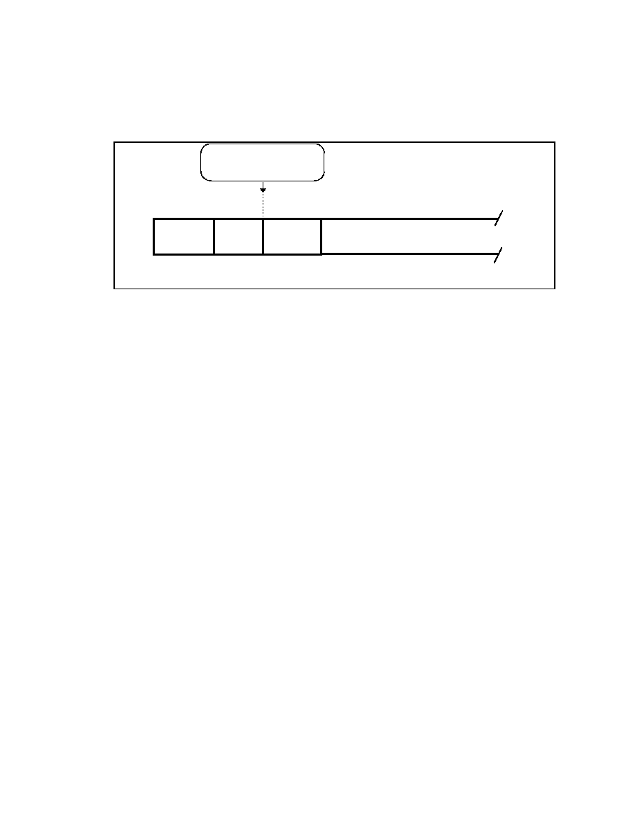
Message Count, bits 0 - 3
The four Message Count bits control hardware
access to the Line Status Registers and are
unaffected by the Status Register Address bits.
The Message Count bits also indicate the
system message-state. For example, if the
Message Count bits are zero, i.e. the power-up
default, Line Status Register zero is active,
although undefined because no messages have
been sent or received. The Message Count bits
are incremented after every active frame. At
point A in Figure 18, for example, the rising
edge of nActive Frame increments Message
Count by one indicating that the first message
has been received; i.e., Line Status Register #1
(status register address 0) is valid, and Line
Status Register #2 is currently active, although
undefined. Hardware prevents the Message
Count register from exceeding eight
('1000'Binary). NOTE: IrDA messages beyond
eight frames are ignored.
nActive Frame
Message Count (0000)
0001
A
0010
0011
FIGURE 18 - MESSAGE COUNT EXAMPLE
32
Bus Status Register (Address 6)
FIFO Indicators (read-only)
The FIFO Indicators reflect the current status of
the SCE FIFO.
FIFO Not Empty, bit 7
The FIFO Not Empty bit when set to one
indicates that there is data in the SCE FIFO.
FIFO Full, bit 6
The FIFO Full bit when set to one indicates that
there is no room for data in the SCE FIFO.
Time-Out, bit 5
The Time-Out bit is the IOCHRDY time-out error
bit. The Time-Out bit when set to one indicates
that an IOCHRDY time-out error has occurred.
Time-Out is reset by the IrCC System Reset
(see Interface Description) following a read of
the Bus Status register, and following a Master
Reset (see Master Block Control Register).
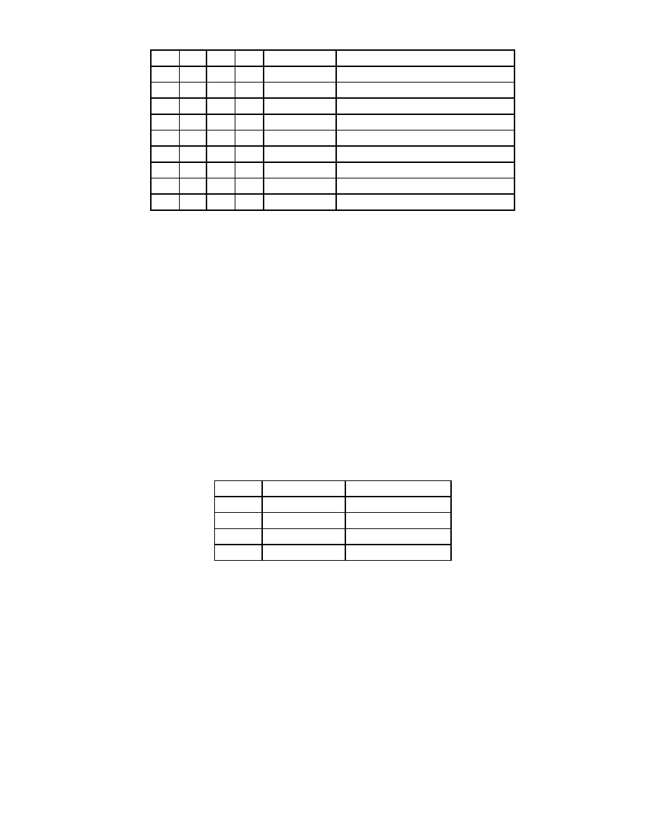
REGISTER BLOCK ONE
Register Block One contains the SCE control
registers (Table 18). Typically, the controls in
Register Block One are needed to configure the
SCE before message transactions can occur.
Table 18 - Register Block One
Address
Direction
Description
Default
A2
A1
A0
D7
D6
D5
D4
D3
D2
D1
D0
0
0
0
R/W
SCE Configuration Register A
'02'hex
aux
ir
block control
bits
half
duplx
tx po-
larity
rx po-
larity
0
0
1
R/W
SCE Configuration Register B
'00'hex
output mux
bits
loop-
back
lpbck
tx crc
no
wait
string
move
dma
burst
dma
enable
0
1
0
R/W
FIFO Threshold Register
'00'hex
0
1
1
1
0
0
1
0
1
1
1
0
SCE Configuration Register A (Address 0)
Auxiliary IR, bit 7
When the Auxiliary IR bit is one and the active
device is routed through the Output Multiplexer
to the IR Port or the COM Port, the transmit
signal also appears at the Auxiliary Port.
Block Control, bits 3 - 6
The Block Control bits select one of the eight
IrCC operational modes (Table 19). The three
low-order Block Control bits are equivalent to
the IR Mode bits in the chip-level configuration
space of earlier devices; e.g., the FDC37C93X
IR Option Register, Serial Port 2, Logical Device
5, Register 0xF1. Provisions have been made in
legacy devices to accommodate IR Mode
selection through either the chip-level
configuration registers or the IrCC Block Control
bits; i.e., the last write from either source
determines the current mode selection and is
visible in both registers.
33
Table 19 - IrCC Logical Block Controls
D6
D5
D4
D3
MODE
DESCRIPTION
0
0
0
0
COM
16550 UART COM Port (default)
0
0
0
1
IrDA SIR - A
Up to 115.2Kbps, Variable 3/16 Pulse
0
0
1
0
ASK IR
Amplitude Shift Keyed Ir Interface
0
0
1
1
IrDA SIR - B
Up to 115.2Kbps, Fixed 1.6us Pulse
0
1
0
0
IrDA HDLC
Includes.576Mbps & 1.152Mbps
0
1
0
1
IrDA4PPM
Includes 4Mbps
0
1
1
0
CONSUMER
TV Remote
0
1
1
1
RAW IR
Direct IR Diode Control
1
X
X
X
OTHER
Reserved
Half Duplex, bit 2
When Half Duplex is zero (default), the 16550A
is in full duplex mode. The Half Duplex bit only
supports the 16550A UART; i.e., this bit has no
effect on the IrCC SCE. The Half Duplex bit is
analogous to the chip-level configuration
register Half Duplex bit and has the same affect
on the UART. Provisions must be made in
legacy devices to accommodate Half Duplex
selection through either the chip-level
configuration registers or the IrCC Half Duplex
bit; i.e., the last write from either source
determines the current mode selection and is
visible in both registers.
Tx/Rx Polarity Bits, 0 - 1
The Tx and Rx Polarity bits define the active
states for signals entering and exiting the Output
Multiplexer ports. IrCC Active states are
typically decoded as zero. The Tx Polarity bit
default is one; the Rx Polarity bit default is zero.
For backward compatibility, the Tx and Rx
Polarity bits do not apply to COM mode; i.e.,
when the Block Control bits are zero. The
relationship between the Output Multiplexer port
signals and the Polarity bits is an exclusive-or
(Table 20). For example, if the IRRx pin in the
Output Multiplexer is one and the Rx Polarity bit
is zero, the signal is inactive and therefore
decoded as a one. The IrCC Tx Polarity bit (bit
1) is equivalent to the Transmit Polarity bit in the
chip-level configuration space of earlier devices;
e.g., the FDC37C93X IR Option Register, Serial
Port 2, Logical Device 5, Register 0xF1. The Rx
Polarity bit (bit 0) is equivalent to the Receive
Polarity bit in the same register. Provisions
have been made in legacy devices to
accommodate Polarity bit selection through
either the chip-level configuration registers or
the SCE registers; i.e., the last write from either
source determines the current Polarity bit value
and is visible in both registers.
Table 20 - Tx/Rx Polarity Bit Effects
SIGNAL
POLARITY BIT
DECODED SIGNAL
0
0
0
0
1
1
1
0
1
1
1
0
34
SCE Configuration Register B (Address 1)
Output Mux, bits 7 - 6
The Output Mux bits select the Output
Multiplexer port for the active encoder/decoder
(Table 21). Inactive outputs depend on the state
of the Tx Polarity bit when the Output Mux bits
are both high, otherwise inactive outputs are
always low. The Output Mux bits are equivalent
to the 93X IR Option Register bits 6-7. The IR
Location Mux, bit 6, in the 93X IR Option
Register is equivalent to Output Mux bit, D6; Bit
7 (Reserved) in the 93X IR Option Register is
equivalent to Output Mux bit, D7. Provisions
have been made in legacy devices to
accommodate Output Multiplexer port selection
through either the chip-level configuration
registers or the Output Mux bits; i.e., the last
write from either source determines the current
port selection and is visible in both registers.
Table 21 - IrCC Output Multiplexer
D7
D6
MUX. MODE
0
0
Active Device to COM Port (default)
0
1
Active Device to IR Port
1
0
Active Device to AUX Port
1
1
Outputs Inactive
Loopback, bit 5
The Loopback bit configures the FIFO and
enables the transmitter/receiver for loopback
testing. The SCE MODES bits must be set to
zero before activating the Loopback bit. When
the Loopback bit is one, the SCE enters a full-
duplex mode with internal loopback capability
for testing. The CRC generator can be
selectively reconfigured for either transmit or
receive. The 128-byte FIFO input is connected
to the SCE receiver output, the FIFO output is
connected to the SCE transmit input. For IrDA
FIR loopback tests the Loopback bit must be set
to zero to exit loopback mode. Consumer IR
loopback tests reset the Loopback bit
automatically when the Rx Data Size register
reaches zero. Provisions must be made
following loopback tests in all modes to verify
the Rx message data in the FIFO.
Loopback Transmit CRC, bit 4
When the Loopback Transmit CRC bit is set to
one, the CRC generator is used by the
transmitter during loopback testing regardless of
the state of the CRC Select bit. Otherwise, the
CRC generator is connected to the receiver
(Table 22).
Table 22 - Hardware CRC Programming
LOOPBACK
BIT
CRC
SELECT
LOOPBACK TX
CRC BIT
HARDWARE DESCRIPTION
0
0
X
No CRC Generation, No CRC Checking
0
1
X
CRC Generation., CRC Checking
1
0
0
No CRC Generation, No CRC Checking
1
0
1
CRC Generation, No CRC Checking
1
1
0
CRC Checking, No CRC Generation
1
1
1
CRC Generation, No CRC Checking

35
No Wait, bit 3
When the No Wait bit is one, the ISA Bus
nSRDY signal goes active following the trailing
edge of the ISA I/O command and inactive
following the rising edge (see Zero Wait State
Support).
String Move, Bit 2
When the String Move bit is one, the
programmed I/O host interface is qualified by
IOCHRDY (Table 23). See IOCHRDY Time-
Out.
DMA Burst Mode, bit 1
When the DMA Burst Mode bit is one, DMA
Burst (Demand) mode is enabled. When the
DMA Burst Mode bit is zero, Single Byte DMA
mode is enabled (Table 23).
DMA Enable, bit 0
DMA Enable is connected to a signal in the
Interface Description called DMAEN that is used
by the chip-level interface to tristate the IrCC
DMA controls when the DMA interface is
inactive. When the DMA Enable bit is one, the
DMA host interface is active (Table 23). When
the DMA Enable bit is zero (default), the nDACK
and TC inputs are disabled and DRQ output is
gated off.
Table 23 - I/O Interface Modes
STRING
MOVE
DMA
BURST
DMA
ENABLE
FUNCTION
0
X
0
Programmed I/O, no IOCHRDY
1
X
0
Programmed I/O, uses IOCHRDY
X
0
1
Single Byte DMA Mode
X
1
1
Demand Mode DMA
FIFO Threshold Register (Address 2)
The FIFO Threshold Register contains the
programmable FIFO threshold count. The FIFO
Threshold is programmable from 0 to 127. Bit 7
in the FIFO Threshold register is read-only and
will always return zero. FIFO Threshold values
typically reflect the overall I/O performance
characteristics of the host; the lower the value,
the longer the interval between service requests
and the faster the host must be to successfully
service them. The same threshold value can be
used for both I/O read and I/O write cases.
36
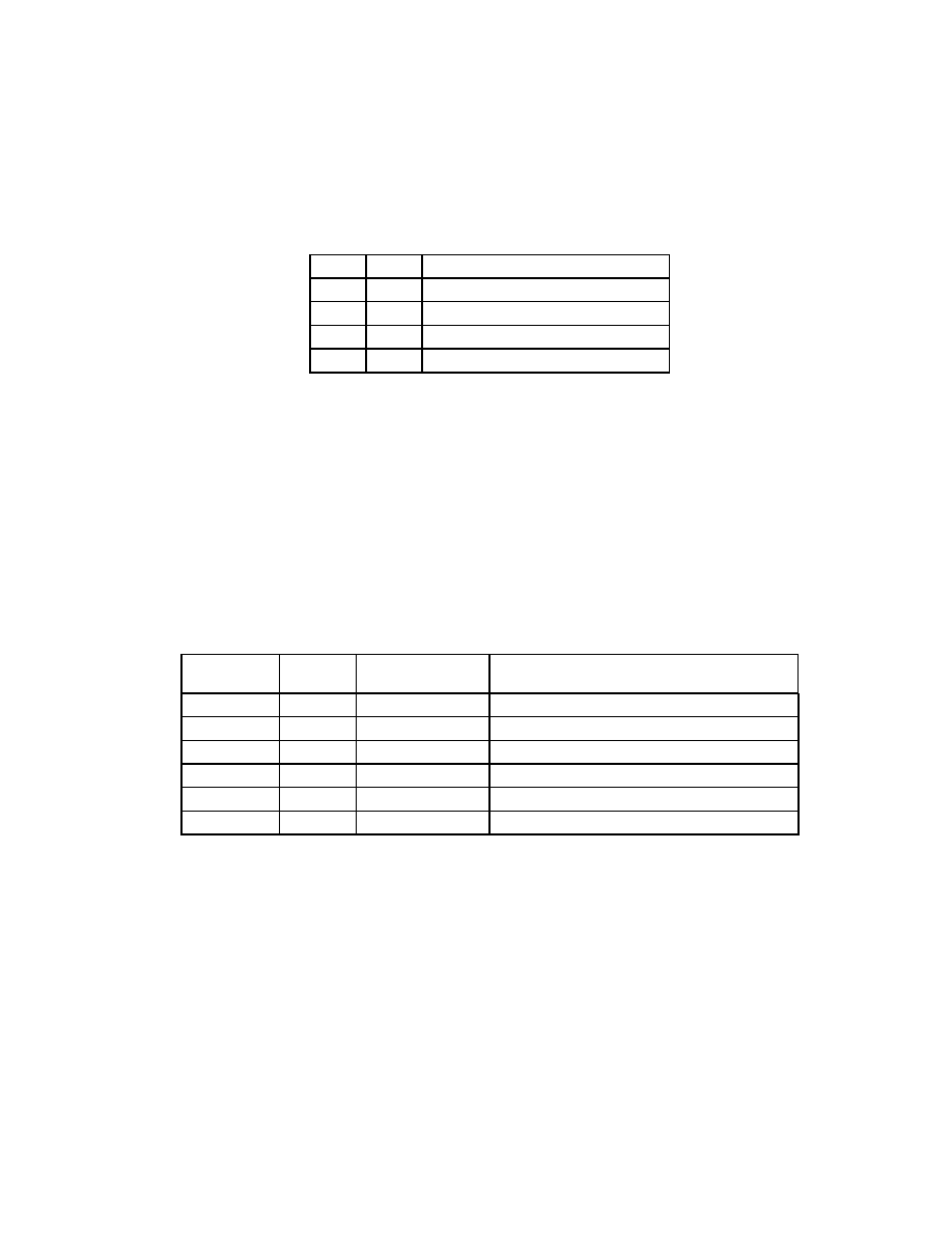
REGISTER BLOCK TWO
Register Block Two contains the Consumer IR
(TV Remote) encoder/decoder configuration
registers (Table 24).
Table 24 - Register Block Two
Address
Direction
Description
Default
A2
A1
A0
D7
D6
D5
D4
D3
D2
D1
D0
0
0
0
R/W
Consumer IR (TV Remote) Control Register
'00'hex
sync
bit
carrier
off
carrier range
bits
0
0
1
R/W
Consumer IR Carrier Rate Register
'29'hex
0
1
0
R/W
Consumer IR Bit Rate Register
'37'hex
0
1
1
1
0
0
1
0
1
1
1
0
Consumer IR Control Register (Address 0)
Sync Bit, bit 7
The Sync Bit enables the receiver bit-rate clock
synchronization mechanisim. When the Sync
bit is one, receiver edge synchronization is
enabled.
Carrier Off, bit 2
The Carrier Off bit bypasses the Consumer IR
Carrier generator/receiver. When the Carrier Off
bit is one, the transmitter outputs a non-
modulated SCE NRZ serial data stream at the
programmed bit rate. Also, when the Carrier Off
bit is one, the receiver does not attempt to
demodulate a carrier from the incoming data
stream and samples the state of the PIN diode
at the programmed bit rate.
Carrier Range, bits 0 - 1
The Consumer IR Carrier Range Bits set the
carrier detect sensitivity of the receiver. The
effects of this register are shown in Table 11 -
Receive Carrier Sense Range.
Consumer IR Carrier Rate Register
(Address 1)
The Consumer IR Carrier Rate Register
programs the ASK carrier frequency divider.
The effects of this register are shown in Table 9-
Representative Carrier Frequencies.
Consumer IR Bit Rate Register (Address2)
The Consumer IR Bit Rate Register programs
the transmit and receive bit-rate divider. The
effects of this register are shown in Table 10 -
Representative Bit Rates.
37
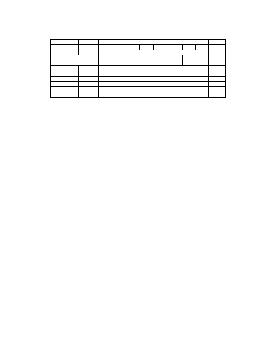
REGISTER BLOCK THREE
Register Block Three contains the IrCC Block
Identifier Registers. These read-only registers
classify the hardware Manufacturer, the Device
ID, the Version number, and Host interface
parameters.
Table 25 - Register Block Three
Address
Direction
Description
Default
A2
A1
A0
D7
D6
D5
D4
D3
D2
D1
D0
0
0
0
RO
SMSC ID (high-byte)
'10'hex
0
0
1
RO
SMSC ID (low-byte)
'B8'hex
0
1
0
RO
CHIP ID
'F1'hex
0
1
1
RO
VERSION Number
'01'hex
1
0
0
RO
IRQ Level
DMA Channel
1
0
1
1
1
0
SMSC ID (Addresses 0 - 1)
The SMSC ID registers contain a 16-bit
manufacturer identification code. Address zero
contains the high byte of this code, address one
contains the low byte.
Chip ID (Address 2)
The Chip ID register specifically identifies this
SMSC product.
Version Number (Address 3)
The Version Number register identifies the
revision-level of the product referenced by the
Chip ID register.
IRQ Level/ DMA Channel (Address 4)
IRQ Level, bits 4 - 7
The IRQ Level bits identify the current active
IRQ number for this device. The value comes
from the 4-bit IRQ Level Bus found in the
Interface description.
DMA Channel, bits 0 - 3
The DMA Channel bits identify the current active
DMA Channel number for this device. The value
comes from the 4-bit DMA Channel Bus found in
the Interface description.
38
REGISTER BLOCK FOUR
Register Block Four contains the IrDA control
registers. These registers control the IrDA
message framing parameters, HDLC clock
speed, and hardware CRC selection. The
registers are read/write.
Table 26 - SCE Register Block Four
Address
Direction
Description
Default
A2
A1
A0
D7
D6
D5
D4
D3
D2
D1
D0
0
0
0
R/W
IrDA Control Register
'C0'hex
1.152
select
crc
select
bof count
(high nibble)
0
0
1
R/W
bof count (low byte)
'00'hex
0
1
0
R/W
brick wall count (low byte)
'00'hex
0
1
1
R/W
brick wall count (high nibble)
tx data size (high nibble)
'00'hex
1
0
0
R/W
tx data size (low byte)
'00'hex
1
0
1
R/W
rx data size (high nibble)
'00'hex
1
1
0
R/W
rx data size (low byte)
'00'hex
IrDA Control Register/BOF Count High
(Address 0)
1.152 Select, bit 7
When the 1.152 Select bit is one, the IrDA
1.152Mbps HDLC-type FIR data rate is selected.
Otherwise the .576Mbps rate is chosen. This bit
only applies to the SCE clock when the Block
Control bits select Mode 2, IrDA HDLC.
CRC Select, bit 6
When the CRC Select bit is one, a hardware-
generated CRC is appended to the frame
payload data during IrDA FIR message
transactions (Table 22).
BOF Count High, bits 0 - 3
The BOF Count specifies the number of
additional flags that are used in a BOF
sequence. For example, at 1.152Mbps, insert
the BOF Count number of additional flag
characters ('7E'hex) at the start of every frame,
excluding brick walled frames. At 4Mbps insert
the BOF Count number of additional PA bytes at
the start of every frame, excluding brick walled
frames. The BOF Count is a 12-bit value. This
register, BOF Count High, is the BOF Count
upper nibble.
BOF Count Low (Address 1)
The BOF Count Low register is the lower byte of
the BOF Count.
Brick Wall Count Low (Address 2)
The Brick Wall Count register specifies the
number of additional interframe padding flags
used for brick walled messages. The Brick Wall
Count is a 12-bit value. The Brick Wall Count
Low register is the Brick Wall Count lower byte.
BW Count High/Tx Data Size High
(Address 3)
Brick Wall Count High, bits 4 - 7
The BW Count High register is the upper nibble
of the Brick Wall Count.
Tx Data Size High, bits 0 - 3
The Tx Data Size register specifies the IrLAP-
negotiated maximum number of payload data
bytes per IrDA transmit message frame if
software CRC is selected, or the IrLAP-
negotiated maximum number of payload data
bytes minus the number of CRC bytes if
hardware CRC is selected. This register is used

39
to 1) constrain the transmitter to a valid IrDA
frame size, 2) simplify multi-frame windowing
for transmit data blocks that are larger than the
maximum packet size and, 3) constrain the SCE
transmitter during loopback testing. NOTE: only
the Tx Data Size register is used for IrDA FIR
loopback testing; only the Rx Data Size register
is required for Consumer IR loopback tests. If
the Tx Data Size register is zero, the IrDA
transmit message size is unlimited; i.e., the
transmitter will operate until the FIFO is empty.
The Tx Data Size High register is the Tx Data
Size high nibble.
Tx Data Size Low (Address 4)
The Tx Data Size Low register is the Tx Data
Size low byte.
Rx Data Size High (Address 5)
Rx Data Size High, bits 0 - 3
The Rx Data Size register specifies the IrLAP-
negotiated maximum number of payload data
bytes per IrDA receive message frame. This
register is used to check each IrDA FIR receive
frame for valid data size and to constrain the
SCE receiver during Consumer IR loopback
testing. NOTE: only the Rx Data Size register is
required for Consumer IR loopback tests; only
the Tx Data Size register is required for IrDA FIR
loopback tests. For Consumer IR loopback
tests, program the Rx Data Size register with
Test_byte_count_1. If the Rx Data Size register
is zero the IrDA receive message size is
unlimited; i.e., a size error cannot occur
because frame size checking is disabled. The
Rx Data Size High register is the Rx Data Size
high nibble.
Rx Data Size Low (Address 6)
The Rx Data Size Low register is the RxData
Size low byte.

40
ACE UART
The SMSC IrCC incorporates one full function
UART compatible with the NS16450, the 16450
ACE registers and the NS16550A. The UART
performs serial-to-parallel conversion on
received characters and parallel-to-serial
conversion on transmit characters. The data
rates are independently programmable from
115.2K baud down to 50 baud. The character
options are programmable for 1 start; 1, 1.5 or 2
stop bits; even, odd, sticky or no parity; and
prioritized interrupts. The UART contains a
programmable baud rate generator that is
capable of dividing the input clock or crystal by
a number from 1 to 65535. The UART is also
capable of supporting the MIDI data rate. Refer
to the Configuration Register section of the
SMSC FDC37C669FR, FDC37C93XFR, or
FDC37C957FR data sheet for information on
disabling, power down and changing the base
address of the UART. The interrupt from the
UART is enabled by programming OUT2 of the
UART to a logic "1". OUT2 being a logic "0"
disables the UART's interrupt.
REGISTER DESCRIPTION
Addressing of the accessible registers of the
Serial Port is shown below. The base
addresses of the serial ports are defined by the
configuration registers. The Serial Port registers
are located at sequentially increasing addresses
above these base addresses. The SMSC IrCC
UART register set is described below.
Table 27 - Addressing The Serial Port
DLAB*
A2
A1
A0
REGISTER NAME
0
0
0
0
Receive Buffer (read)
0
0
0
0
Transmit Buffer (write)
0
0
0
1
Interrupt Enable (read/write)
X
0
1
0
Interrupt Identification (read)
X
0
1
0
FIFO Control (write)
X
0
1
1
Line Control (read/write)
X
1
0
0
Modem Control (read/write)
X
1
0
1
Line Status (read/write)
X
1
1
0
Modem Status (read/write)
X
1
1
1
Scratchpad (read/write)
1
0
0
0
Divisor LSB (read/write)
1
0
0
1
Divisor MSB (read/write
*NOTE: DLAB is Bit 7 of the Line Control Register

41
The following section describes the operation of
the registers.
RECEIVE BUFFER REGISTER (RB)
Address Offset = 0H, DLAB = 0, READ ONLY
This register holds the received incoming data
byte. Bit 0 is the least significant bit, which is
transmitted and received first. Received data is
double buffered; this uses an additional shift
register to receive the serial data stream and
convert it to a parallel 8 bit word which is
transferred to the Receive Buffer register. The
shift register is not accessible.
TRANSMIT BUFFER REGISTER (TB)
Address Offset = 0H, DLAB = 0, WRITE ONLY
This register contains the data byte to be
transmitted. The transmit buffer is double
buffered, utilizing an additional shift register (not
accessible) to convert the 8 bit data word to a
serial format. This shift register is loaded from
the Transmit Buffer when the transmission of
the previous byte is complete.
INTERRUPT ENABLE REGISTER (IER)
Address Offset = 1H, DLAB = 0, READ/WRITE
The lower four bits of this register control the
enables of the five interrupt sources of the Serial
Port interrupt. It is possible to totally disable the
interrupt system by resetting bits 0 through 3 of
this register. Similarly, setting the appropriate
bits of this register to a high, selected interrupts
can be enabled. Disabling the interrupt system
inhibits the Interrupt Identification Register and
disables any Serial Port interrupt out of the
SMSC IrCC. All other system functions operate
in their normal manner, including the Line
Status and MODEM Status Registers. The
contents of the Interrupt Enable Register are
described below.
Bit 0
This bit enables the Received Data Available
Interrupt (and timeout interrupts in the FIFO
mode) when set to logic "1".
Bit 1
This bit enables the Transmitter Holding
Register Empty Interrupt when set to logic "1".
Bit 2
This bit enables the Received Line Status
Interrupt when set to logic "1". The error
sources causing the interrupt are Overrun,
Parity, Framing and Break. The Line Status
Register must be read to determine the source.
Bit 3
This bit enables the MODEM Status Interrupt
when set to logic "1". This is caused when one
of the Modem Status Register bits changes
state.
Bits 4 through 7
These bits are always logic "0".
FIFO CONTROL REGISTER (FCR)
Address Offset = 2H, DLAB = X, WRITE
This is a write only register at the same location
as the IIR. This register is used to enable and
clear the FIFOs, set the RCVR FIFO trigger
level. Note: DMA is not supported.
Bit 0
Setting this bit to a logic "1" enables both the
XMIT and RCVR FIFOs. Clearing this bit to a
logic "0" disables both the XMIT and RCVR
FIFOs and clears all bytes from both FIFOs.
When changing from FIFO Mode to non-FIFO
(16450) mode, data is automatically cleared
from the FIFOs. This bit must be a 1 when
other bits in this register are written to or they
will not be properly programmed.
Bit 1
Setting this bit to a logic "1" clears all bytes in
the RCVR FIFO and resets its counter logic to 0.
The shift register is not cleared. This bit is self-
clearing.

42
Bit 2
Setting this bit to a logic "1" clears all bytes in
the XMIT FIFO and resets its counter logic to 0.
The shift register is not cleared. This bit is self-
clearing.
Bit 3
Writting to this bit has no effect on the operation
of the UART. The RXRDY and TXRDY pins are
not available on this chip.
Bit 4,5
Reserved
BIT 7
BIT 6
RCVR FIFO
TRIGGER LEVEL
0
0
1
0
1
4
1
0
8
1
1
14
Bit 6,7
These bits are used to set the trigger level for
the RCVR FIFO interrupt.
INTERRUPT IDENTIFICATION REGISTER
(IIR)
Address Offset = 2H, DLAB = X, READ
By accessing this register, the host CPU can
determine the highest priority interrupt and its
source. Four levels of priority interrupt exist.
They are in descending order of priority:
1. Receiver Line Status (highest priority)
2. Received Data Ready
3. Transmitter Holding Register Empty
4. MODEM Status (lowest priority)
Information indicating that a prioritized interrupt
is pending and the source of that interrupt is
stored in the Interrupt Identification Register
(refer to Interrupt Control Table). When the
CPU accesses the IIR, the Serial Port freezes all
interrupts and indicates the highest priority
pending interrupt to the CPU. During this CPU
access, even if the Serial Port records new
interrupts, the current indication does not
change until access is completed. The contents
of the IIR are described below.
Bit 0
This bit can be used in either a hardwired
prioritized or polled environment to indicate
whether an interrupt is pending. When bit 0 is a
logic "0", an interrupt is pending and the
contents of the IIR may be used as a pointer to
the appropriate internal service routine. When
bit 0 is a logic "1", no interrupt is pending.
Bits 1 and 2
These two bits of the IIR are used to identify the
highest priority interrupt pending as indicated by
the Interrupt Control Table.
Bit 3
In non-FIFO mode, this bit is a logic "0". In
FIFO mode this bit is set along with bit 2 when a
timeout interrupt is pending.
Bits 4 and 5
These bits of the IIR are always logic "0".
Bits 6 and 7
These two bits are set when the FIFO
CONTROL Register bit 0 equals 1.

43
Table 28 - Interrupt Control Table
FIFO
MODE
ONLY
INTERRUPT
IDENTIFICATION
REGISTER
INTERRUPT SET AND RESET FUNCTIONS
BIT 3
BIT 2
BIT 1
BIT 0
PRIORITY
LEVEL
INTERRUPT
TYPE
INTERRUPT
SOURCE
INTERRUPT
RESET
CONTROL
0
0
0
1
-
None
None
-
0
1
1
0
Highest
Receiver Line
Status
Overrun Error,
Parity Error,
Framing Error
or Break
Interrupt
Reading the
Line Status
Register
0
1
0
0
Second
Received Data
Available
Receiver Data
Available
Read
Receiver
Buffer or the
FIFO drops
below the
trigger level.
1
1
0
0
Second
Character
Timeout
Indication
No Characters
Have Been
Removed From
or Input to the
RCVR FIFO
during the last
4 Char times
and there is at
least 1 char in
it during this
time
Reading the
Receiver
Buffer
Register
0
0
1
0
Third
Transmitter
Holding Register
Empty
Transmitter
Holding
Register Empty
Reading the
IIR Register
(if Source of
Interrupt) or
Writing the
Transmitter
Holding
Register
0
0
0
0
Fourth
MODEM Status
Clear to Send
or Data Set
Ready or Ring
Indicator or
Data Carrier
Detect
Reading the
MODEM
Status
Register

44
LINE CONTROL REGISTER (LCR)
Address Offset = 3H, DLAB = 0, READ/WRITE
This register contains the format information of
the serial line. The bit definitions are:
Bits 0 and 1
These two bits specify the number of bits in
each transmitted or received serial character.
The encoding of bits 0 and 1 is as follows:
BIT 1
BIT 0
WORD LENGTH
0
0
1
1
0
1
0
1
5 Bits
6 Bits
7 Bits
8 Bits
The Start, Stop and Parity bits are not included
in the word length.
Bit 2
This bit specifies the number of stop bits in each
transmitted or received serial character. The
following table summarizes the information.
BIT 2
WORD LENGTH
NUMBER OF
STOP BITS
0
--
1
1
5 bits
1.5
1
6 bits
2
1
7 bits
2
1
8 bits
2
Note: The receiver will ignore all stop bits
beyond the first, regardless of the number used
in transmitting.
Bit 3
Parity Enable bit. When bit 3 is a logic "1", a
parity bit is generated (transmit data) or
checked (receive data) between the last data
word bit and the first stop bit of the serial data.
(The parity bit is used to generate an even or
odd number of 1s when the data word bits and
the parity bit are summed).
Bit 4
Even Parity Select bit. When bit 3 is a logic "1"
and bit 4 is a logic "0", an odd number of logic
"1"'s is transmitted or checked in the data word
bits and the parity bit. When bit 3 is a logic "1"
and bit 4 is a logic "1" an even number of bits is
transmitted and checked.
Bit 5
Stick Parity bit. When bit 3 is a logic "1" and bit
5 is a logic "1", the parity bit is transmitted and
then detected by the receiver in the opposite
state indicated by bit 4.
Bit 6
Set Break Control bit. When bit 6 is a logic "1",
the transmit data output (TXD) is forced to the
Spacing or logic "0" state and remains there
(until reset by a low level bit 6) regardless of
other transmitter activity. This feature enables
the Serial Port to alert a terminal in a
communications system.
Bit 7
Divisor Latch Access bit (DLAB). It must be set
high (logic "1") to access the Divisor Latches of
the Baud Rate Generator during read or write
operations. It must be set low (logic "0") to
access the Receiver Buffer Register, the
Transmitter Holding Register, or the Interrupt
Enable Register.
MODEM CONTROL REGISTER (MCR)
Address Offset = 4H, DLAB = X,
READ/WRITE
This 8 bit register controls the interface with the
MODEM or data set (or device emulating a
MODEM). The contents of the MODEM control
register are described below.

45
Bit 0
This bit controls the Data Terminal Ready
(nDTR) output. When bit 0 is set to a logic "1",
the nDTR output is forced to a logic "0". When
bit 0 is a logic "0", the nDTR output is forced to
a logic "1".
Bit 1
This bit controls the Request To Send (nRTS)
output. Bit 1 affects the nRTS output in a
manner identical to that described above for bit
0.
Bit 2
This bit controls the Output 1 (OUT1) bit. This
bit does not have an output pin and can only be
read or written by the CPU.
Bit 3
Output 2 (OUT2). This bit is used to enable an
UART interrupt. When OUT2 is a logic "0", the
serial port interrupt output is forced to a high
impedance state - disabled. When OUT2 is a
logic "1", the serial port interrupt outputs are
enabled.
Bit 4
This bit provides the loopback feature for
diagnostic testing of the Serial Port. When bit 4
is set to logic "1", the following occur:
1. The TXD is set to the Marking State(logic
"1").
2. The receiver Serial Input (RXD) is
disconnected.
3. The output of the Transmitter Shift Register
is "looped back" into the Receiver Shift
Register input.
4. All MODEM Control inputs (nCTS, nDSR,
nRI and nDCD) are disconnected.
5. The four MODEM Control outputs (nDTR,
nRTS, and OUT2) are internally connected
to the four MODEM Control inputs.
6. The Modem Control output pins are forced
inactive high.
7. Data that is transmitted is immediately
received.
This feature allows the processor to verify the
transmit and receive data paths of the Serial
Port. In the diagnostic mode, the receiver and
the transmitter interrupts are fully operational.
The MODEM Control Interrupts are also
operational but the interrupts' sources are now
the lower four bits of the MODEM Control
Register instead of the MODEM Control inputs.
The interrupts are still controlled by the Interrupt
Enable Register.
Bits 5 through 7
These bits are permanently set to logic zero.
LINE STATUS REGISTER (LSR)
Address Offset = 5H, DLAB = X, READ/
WRITE
Bit 0
Data Ready (DR). It is set to a logic "1"
whenever a complete incoming character has
been received and transferred into the Receiver
Buffer Register or the FIFO. Bit 0 is reset to a
logic "0" by reading all of the data in the Receive
Buffer Register or the FIFO.
Bit 1
Overrun Error (OE). Bit 1 indicates that data in
the Receiver Buffer Register was not read before
the next character was transferred into the
register, thereby destroying the previous
character. In FIFO mode, an overrunn error will
occur only when the FIFO is full and the next
character has been completely received in the
shift register, the character in the shift register is
overwritten but not transferred to the FIFO. The
OE indicator is set to a logic "1" immediately
upon detection of an overrun condition, and
reset whenever the Line Status Register is read.
Bit 2
Parity Error (PE). Bit 2 indicates that the
received data character does not have the
correct even or odd parity, as selected by the
even parity select bit. The PE is set to a logic
"1" upon detection of a parity error and is reset
to a logic "0" whenever the Line Status Register

46
is read. In the FIFO mode this error is
associated with the particular character in the
FIFO it applies to. This error is indicated when
the associated character is at the top of the
FIFO.
Bit 3
Framing Error (FE). Bit 3 indicates that the
received character did not have a valid stop bit.
Bit 3 is set to a logic "1" whenever the stop bit
following the last data bit or parity bit is detected
as a zero bit (Spacing level). The FE is reset to
a logic "0" whenever the Line Status Register is
read. In the FIFO mode this error is associated
with the particular character in the FIFO it
applies to. This error is indicated when the
associated character is at the top of the FIFO.
The Serial Port will try to resynchronize after a
framing error. To do this, it assumes that the
framing error was due to the next start bit, so it
samples this 'start' bit twice and then takes in
the 'data'.
Bit 4
Break Interrupt (BI). Bit 4 is set to a logic "1"
whenever the received data input is held in the
Spacing state (logic "0") for longer than a full
word transmission time (that is, the total time of
the start bit + data bits + parity bits + stop bits).
The BI is reset after the CPU reads the contents
of the Line Status Register. In the FIFO mode
this error is associated with the particular
character in the FIFO it applies to. This error is
indicated when the associated character is at
the top of the FIFO. When break occurs only
one zero character is loaded into the FIFO.
Restarting after a break is received, requires the
serial data (RXD) to be logic "1" for at least 1/2
bit time.
Note: Bits 1 through 4 are the error conditions
that produce a Receiver Line Status Interrupt
whenever any of the corresponding conditions
are detected and the interrupt is enabled.
Bit 5
Transmitter Holding Register Empty (THRE).
Bit 5 indicates that the Serial Port is ready to
accept a new character for transmission. In
addition, this bit causes the Serial Port to issue
an interrupt when the Transmitter Holding
Register interrupt enable is set high. The THRE
bit is set to a logic "1" when a character is
transferred from the Transmitter Holding
Register into the Transmitter Shift Register. The
bit is reset to logic "0" whenever the CPU loads
the Transmitter Holding Register. In the FIFO
mode this bit is set when the XMIT FIFO is
empty, it is cleared when at least 1 byte is
written to the XMIT FIFO. Bit 5 is a read only
bit.
Bit 6
Transmitter Empty (TEMT). Bit 6 is set to a
logic "1" whenever the Transmitter Holding
Register (THR) and Transmitter Shift Register
(TSR) are both empty. It is reset to logic "0"
whenever either the THR or TSR contains a data
character. Bit 6 is a read only bit. In the FIFO
mode this bit is set whenever the THR and TSR
are both empty,
Bit 7
This bit is permanently set to logic "0" in the 450
mode. In the FIFO mode, this bit is set to a
logic "1" when there is at least one parity error,
framing error or break indication in the FIFO.
This bit is cleared when the LSR is read if there
are no subsequent errors in the FIFO.
MODEM STATUS REGISTER (MSR)
Address Offset = 6H, DLAB = X, READ/
WRITE
This 8 bit register provides the current state of
the control lines from the MODEM (or peripheral
device). In addition to this current state
information, four bits of the MODEM Status
Register (MSR) provide change information.

47
These bits are set to logic "1" whenever a
control input from the MODEM changes state.
They are reset to logic "0" whenever the
MODEM Status Register is read.
Bit 0
Delta Clear To Send (DCTS). Bit 0 indicates
that the nCTS input to the chip has changed
state since the last time the MSR was read.
Bit 1
Delta Data Set Ready (DDSR). Bit 1 indicates
that the nDSR input has changed state since
the last time the MSR was read.
Bit 2
Trailing Edge of Ring Indicator (TERI). Bit 2
indicates that the nRI input has changed from
logic "0" to logic "1".
Bit 3
Delta Data Carrier Detect (DDCD). Bit 3
indicates that the nDCD input to the chip has
changed state.
Note: Whenever bit 0, 1, 2, or 3 is set to a logic
"1", a MODEM Status Interrupt is generated.
Bit 4
This bit is the complement of the Clear To Send
(nCTS) input. If bit 4 of the MCR is set to logic
"1", this bit is equivalent to nRTS in the MCR.
Bit 5
This bit is the complement of the Data Set
Ready (nDSR) input. If bit 4 of the MCR is set
to logic "1", this bit is equivalent to DTR in the
MCR.
Bit 6
This bit is the complement of the Ring Indicator
(nRI) input. If bit 4 of the MCR is set to logic
"1", this bit is equivalent to OUT1 in the MCR.
Bit 7
This bit is the complement of the Data Carrier
Detect (nDCD) input. If bit 4 of the MCR is set
to logic "1", this bit is equivalent to OUT2 in the
MCR.
SCRATCHPAD REGISTER (SCR)
Address Offset =7H, DLAB =X, READ/WRITE
This 8 bit read/write register has no effect on the
operation of the Serial Port. It is intended as a
scratchpad register to be used by the
programmer to hold data temporarily.
PROGRAMMABLE BAUD RATE GENERATOR
(AND DIVISOR LATCHES DLH, DLL)
The Serial Port contains a programmable Baud
Rate Generator that is capable of taking any
clock input (DC to 3 MHz) and dividing it by any
divisor from 1 to 65535. This output frequency
of the Baud Rate Generator is 16x the Baud
rate. Two 8 bit latches store the divisor in 16 bit
binary format. These Divisor Latches must be
loaded during initialization in order to insure
desired operation of the Baud Rate Generator.
Upon loading either of the Divisor Latches, a 16
bit Baud counter is immediately loaded. This
prevents long counts on initial load. If a 0 is
loaded into the BRG registers the output divides
the clock by the number 3. If a 1 is loaded the
output is the inverse of the input oscillator. If a
two is loaded the output is a divide by 2 signal
with a 50% duty cycle. If a 3 or greater is
loaded the output is low for 2 bits and high for
the remainder of the count. The input clock to
the BRG is the 24 MHz crystal divided by 13,
giving a 1.8462 MHz clock.
Table 29 shows the baud rates possible with a
1.8462 MHz crystal.

48
Effect Of The Reset on Register File
The Reset Function Table (Table 30) details the
effect of the Reset input on each of the registers
of the Serial Port.
FIFO INTERRUPT MODE OPERATION
When the RCVR FIFO and receiver interrupts
are enabled (FCR bit 0 = "1", IER bit 0 = "1"),
RCVR interrupts occur as follows:
A. The receive data available interrupt will be
issued when the FIFO has reached its
programmed trigger level; it is cleared as
soon as the FIFO drops below its
programmed trigger level.
B. The IIR receive data available indication
also occurs when the FIFO trigger level is
reached. It is cleared when the FIFO drops
below the trigger level.
C. The receiver line status interrupt (IIR=06H),
has higher priority than the received data
available (IIR=04H) interrupt.
D. The data ready bit (LSR bit 0)is set as soon
as a character is transferred from the shift
register to the RCVR FIFO. It is reset when
the FIFO is empty.
When RCVR FIFO and receiver interrupts are
enabled, RCVR FIFO timeout interrupts occur
as follows:
A. A FIFO timeout interrupt occurs if all the
following conditions exist:
-
at least one character is in the FIFO
-
The most recent serial character
received was longer than 4 continuous
character times ago. (If 2 stop bits are
programmed, the second one is
included in this time delay.)
-
The most recent CPU read of the FIFO
was longer than 4 continuous character
times ago.
-
This will cause a maximum character
received to interrupt issued delay of
160 msec at 300 BAUD with a 12 bit
character.
B. Character times are calculated by using the
RCLK input for a clock signal (this makes
the delay proportional to the baudrate).
C. When a timeout interrupt has occurred it is
cleared and the timer reset when the CPU
reads one character from the RCVR FIFO.
D. When a timeout interrupt has not occurred
the timeout timer is reset after a new
character is received or after the CPU reads
the RCVR FIFO.
When the XMIT FIFO and transmitter interrupts
are enabled (FCR bit 0 = "1", IER bit 1 = "1"),
XMIT interrupts occur as follows:
A. The transmitter holding register interrupt
(02H) occurs when the XMIT FIFO is empty;
it is cleared as soon as the transmitter
holding register is written to (1 of 16
characters may be written to the XMIT FIFO
while servicing this interrupt) or the IIR is
read.
B. The transmitter FIFO empty indications will
be delayed 1 character time minus the last
stop bit time whenever the following occurs:
THRE=1 and there have not been at least
two bytes at the same time in the transmitte
FIFO since the last THRE=1. The
transmitter interrupt after changing FCR0
will be immediate, if it is enabled.
Character timeout and RCVR FIFO trigger level
interrupts have the sme priority as the current
received data available interrupt; XMIT FIFO
empty has the same priority as the current
transmitter holding register empty interrupt.
FIFO POLLED MODE OPERATION
With FCR bit 0 = "1" resetting IER bits 0, 1, 2 or
3 or all to zero puts the UART in the FIFO
Polled Mode of operation. Since the RCVR and
are controlled separately, either one or both can
be in the polled mode of operation.

49
In this mode, the user's program will check
RCVR and XMITTER status via the LSR. LSR
definitions for the FIFO Polled Mode are as
follows:
-
Bit 0=1 as long as there is one byte in the
RCVR FIFO.
-
Bits 1 to 4 specify which error(s) have
occurred. Character error status is handled
the same way as when in the
interruptmode, the IIR is not affected since
EIR bit 2=0.
-
Bit 5 indicates when the XMIT FIFO is
empty.
-
Bit 6 indicates that both the XMIT FIFO and
shift register are empty.
-
Bit 7 indicates whether there are any errors
in the RCVR FIFO.
There is no trigger level reached or timeout
condition indicated in the FIFO Polled Mode,
however, the RCVR and XMIT FIFOs are still
fully capable of holding characters.
Table 29 - Baud Rates Using 1.8462 MHz Clock (24 MHz/13)
DESIRED
BAUD RATE
DIVISOR USED TO
GENERATE 16X CLOCK
PERCENT ERROR DIFFERENCE
BETWEEN DESIRED AND ACTUAL*
CRC:
BIT 7 OR 6
50
2304
0.001
X
75
1536
-
X
110
1047
-
X
134.5
857
0.004
X
150
768
-
X
300
384
-
X
600
192
-
X
1200
96
-
X
1800
64
-
X
2000
58
0.005
X
2400
48
-
X
3600
32
-
X
4800
24
-
X
7200
16
-
X
9600
12
-
X
19200
6
-
X
38400
3
0.030
X
57600
2
0.16
X
115200
1
0.16
X
230400
32770
0.16
1
460800
32769
0.16
1
*NOTE: The percentage error for all baud rates, except where indicated otherwise, is 0.2%.

50
Table 30 - Reset Function Table
REGISTER/SIGNAL
RESET CONTROL
RESET STATE
Interrupt Enable Register
RESET
All bits low
Interrupt Identification Reg.
RESET
Bit 0 is high; Bits 1 thru 7 low
FIFO Control
RESET
All bits low
Line Control Reg.
RESET
All bits low
MODEM Control Reg.
RESET
All bits low
Line Status Reg.
RESET
All bits low except 5, 6 high
MODEM Status Reg.
RESET
Bits 0 - 3 low; Bits 4 - 7 input
TXD1, TXD2
RESET
High
INTRPT (RCVR errs)
RESET/Read LSR
Low
INTRPT (RCVR Data Ready)
RESET/Read RBR
Low
INTRPT (THRE)
RESET/ReadIIR/Write THR
Low
OUT2B
RESET
High
RTSB
RESET
High
DTRB
RESET
High
OUT1B
RESET
High
RCVR FIFO
RESET/FCR1*FCR0/_FCR0
All Bits Low
XMIT FIFO
RESET/FCR1*FCR0/_FCR0
All Bits Low

51
Table 31 - Register Summary For An Individual UART Channel
REGISTER
ADDRESS*
REGISTER NAME
REGISTER
SYMBOL
BIT 0
BIT 1
ADDR = 0
DLAB = 0
Receive Buffer Register (Read Only)
RBR
Data Bit 0
(Note 1)
Data Bit 1
ADDR = 0
DLAB = 0
Transmitter Holding Register (Write
Only)
THR
Data Bit 0
Data Bit 1
ADDR = 1
DLAB = 0
Interrupt Enable Register
IER
Enable
Received
Data
Available
Interrupt
(ERDAI)
Enable
Transmitter
Holding
Register
Empty
Interrupt
(ETHREI)
ADDR = 2
Interrupt Ident. Register (Read Only)
IIR
"0" if Interrupt
Pending
Interrupt ID
Bit
ADDR = 2
FIFO Control Register (Write Only)
FCR
FIFO Enable
RCVR FIFO
Reset
ADDR = 3
Line Control Register
LCR
Word Length
Select Bit 0
(WLS0)
Word Length
Select Bit 1
(WLS1)
ADDR = 4
MODEM Control Register
MCR
Data
Terminal
Ready (DTR)
Request to
Send (RTS)
ADDR = 5
Line Status Register
LSR
Data Ready
(DR)
Overrun
Error (OE)
ADDR = 6
MODEM Status Register
MSR
Delta Clear to
Send (DCTS)
Delta Data
Set Ready
(DDSR)
ADDR = 7
Scratch Register (Note 4)
SCR
Bit 0
Bit 1
ADDR = 0
DLAB = 1
Divisor Latch (LS)
DDL
Bit 0
Bit 1
ADDR = 1
DLAB = 1
Divisor Latch (MS)
DLM
Bit 8
Bit 9
*DLAB is Bit 7 of the Line Control Register (ADDR = 3).
Note 1: Bit 0 is the least significant bit. It is the first bit serially transmitted or received.
Note 2: When operating in the XT mode, this bit will be set any time that the transmitter shift register is empty.

52
Table 31 - Register Summary For An Individual UART Channel (continued)
BIT 2
BIT 3
BIT 4
BIT 5
BIT 6
BIT 7
Data Bit 2
Data Bit 3
Data Bit 4
Data Bit 5
Data Bit 6
Data Bit 7
Data Bit 2
Data Bit 3
Data Bit 4
Data Bit 5
Data Bit 6
Data Bit 7
Enable
Receiver Line
Status
Interrupt
(ELSI)
Enable
MODEM
Status
Interrupt
(EMSI)
0
0
0
0
Interrupt ID
Bit
Interrupt ID
Bit (Note 5)
0
0
FIFOs
Enabled
(Note 5)
FIFOs
Enabled
(Note 5)
XMIT FIFO
Reset
DMA Mode
Select (Note
6)
Reserved
Reserved
RCVR Trigger
LSB
RCVR Trigger
MSB
Number of
Stop Bits
(STB)
Parity Enable
(PEN)
Even Parity
Select (EPS)
Stick Parity
Set Break
Divisor Latch
Access Bit
(DLAB)
OUT1
(Note 3)
OUT2
(Note 3)
Loop
0
0
0
Parity Error
(PE)
Framing Error
(FE)
Break
Interrupt (BI)
Transmitter
Holding
Register
(THRE)
Transmitter
Empty
(TEMT) (Note
2)
Error in
RCVR FIFO
(Note 5)
Trailing Edge
Ring Indicator
(TERI)
Delta Data
Carrier Detect
(DDCD)
Clear to Send
(CTS)
Data Set
Ready (DSR)
Ring Indicator
(RI)
Data Carrier
Detect (DCD)
Bit 2
Bit 3
Bit 4
Bit 5
Bit 6
Bit 7
Bit 2
Bit 3
Bit 4
Bit 5
Bit 6
Bit 7
Bit 10
Bit 11
Bit 12
Bit 13
Bit 14
Bit 15
Note 3: This bit no longer has a pin associated with it.
Note 4: When operating in the XT mode, this register is not available.
Note 5: These bits are always zero in the non-FIFO mode.
Note 6: Writing a one to this bit has no effect. DMA modes are not supported in this chip.

53
NOTES ON SERIAL PORT OPERATION
FIFO MODE OPERATION:
GENERAL
The RCVR FIFO will hold up to 16 bytes
regardless of which trigger level is selected.
TX AND RX FIFO OPERATION
The Tx portion of the UART transmits data
through TXD as soon as the CPU loads a byte
into the Tx FIFO. The UART will prevent
loads to the Tx FIFO if it currently holds 16
characters. Loading to the Tx FIFO will again
be enabled as soon as the next character is
transferred to the Tx shift register. These
capabilities account for the largely autonomous
operation of the Tx.
The UART starts the above operations typically
with a Tx interrupt. The chip issues a Tx
interrupt whenever the Tx FIFO is empty and the
Tx interrupt is enabled, except in the following
instance. Assume that the Tx FIFO is empty
and the CPU starts to load it. When the first
byte enters the FIFO the Tx FIFO empty
interrupt will transition from active to inactive.
Depending on the execution speed of the service
routine software, the UART may be able to
transfer this byte from the FIFO to the shift
register before the CPU loads another byte. If
this happens, the Tx FIFO will be empty again
and typically the UART's interrupt line would
transition to the active state. This could cause a
system with an interrupt control unit to record a
Tx FIFO empty condition, even though the CPU
is currently servicing that interrupt. Therefore,
after the first byte has been loaded into the
FIFO the UART will wait one serial character
transmission time before issuing a new Tx
FIFO empty interrupt.
This one character Tx interrupt delay will
remain active until at least two bytes have
been loaded into the FIFO, concurrently.
When the Tx FIFO empties after this
condition, the Tx interrupt will be activated
without a one character delay.
Rx support functions and operation are quite
different from those described for the
transmitter. The Rx FIFO receives data until the
number of bytes in the FIFO equals the selected
interrupt trigger level. At that time if Rx
interrupts are enabled, the UART will issue an
interrupt to the CPU. The Rx FIFO will continue
to store bytes until it holds 16 of them. It will
not accept any more data when it is full. Any
more data entering the Rx shift register will set
the Overrun Error flag. Normally, the FIFO
depth and the programmable trigger levels will
give the CPU ample time to empty the Rx FIFO
before an overrun occurs.
One side-effect of having a Rx FIFO is that the
selected interrupt trigger level may be above the
data level in the FIFO. This could occur when
data at the end of the block contains fewer bytes
than the trigger level. No interrupt would be
issued to the CPU and the data would remain in
the UART. To prevent the software from
having to check for this situation the chip
incorporates a timeout interrupt.
The timeout interrupt is activated when there is
a least one byte in the Rx FIFO, and neither the
CPU nor the Rx shift register has accessed the
Rx FIFO within 4 character times of the last
byte. The timeout interrupt is cleared or reset
when the CPU reads the Rx FIFO or another
character enters it.
These FIFO related features allow optimization
of CPU/UART transactions and are especially
useful given the higer baud rate capability (256
kbaud).
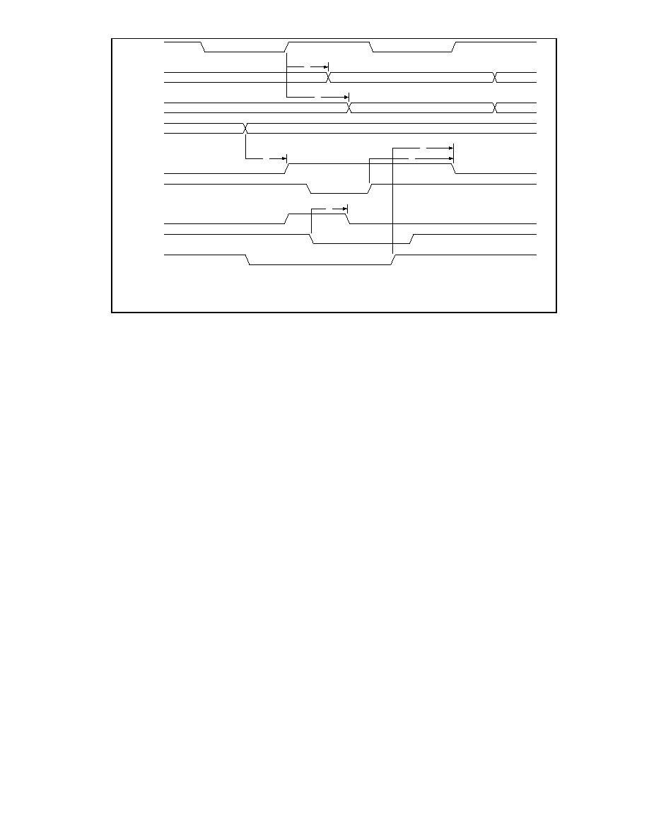
54
t1
t5
t2
t4
t6
t3
nIOW
nRTSx,
nDTRx
IRQx
nCTSx,
nDSRx,
nDCDx
IRQx
nIOW
IRQx
nIOR
nRIx
FIGURE 19 - SERIAL PORT TIMING

55
SCE
DESCRIPTION
The SCE is a half-duplex synchronous serial
communications controller that controls data
flow between the Bus Interface I/O block and the
IrDA FIR and Consumer IR (TV Remote)
Encoders (Figure 20). The SCE also includes
partial full-duplex loopback functionality for
diagnostic testing. Bit rates from .4Kbps to
4Mbps are supported. All of the SCE register
controls are located in the nSCE-addressable 8-
bit Register Blocks.
FRAMING
The SCE operates with and without framing.
With framing implies that the SCE works with
the IrDA FIR encoder/decoder so the required
symbols for the non-payload data portions of the
.576Mbps, 1.152Mbps and 4Mbps packets can
be generated. Without framing implies that the
SCE acts simply as serial-to-parallel converter
for the Consumer IR (TV Remote) encoder/
decoder.
ACTIVE FRAME INDICATOR
The SCE signal nActiveFrame is a PLA state
variable that is synchronized to both IrDA FIR
and Consumer IR message frames.
nActiveFrame cycles high and low for each
message frame, regardless of the state of the
Brick Wall bit. nActiveFrame is primarily used
to trigger active frame interrupts and to advance
the Message Count bits that control hardware
access to the Line Status Registers.
IrDA Modes
Transmit
nActiveFrame goes active as soon as the IrDA
transmitter initiates a BOF sequence.
nActiveFrame becomes inactive as soon as the
IrDA transmitter completes an EOF sequence.
In the case of a transmit abort, nActiveFrame
becomes inactive as soon as the IrDA
transmitter completes the abort sequence.
Receive
nActiveFrame goes active as soon as the IrDA
receiver detects valid payload data; i.e., after a
valid BOF sequence. nActiveFrame becomes
inactive as soon as the IrDA receiver detects an
EOF sequence. In the case of a FIFO Overrun
or abort, nActiveFrame becomes inactive as
soon as the IrDA receiver updates the status
register and signals the End of Message.
Serial-to-Parallel
Converter
Parallel-to-Serial
Converter
16/32-bit
CRC Generator
16/32-bit
CRC Checker
8
1
8
1
Timing
&
Control
Transmit
Receive
Controls
FIR/TV
Encoder
FIR/TV
Decoder
FIGURE 20 - SCE BLOCK DIAGRAM
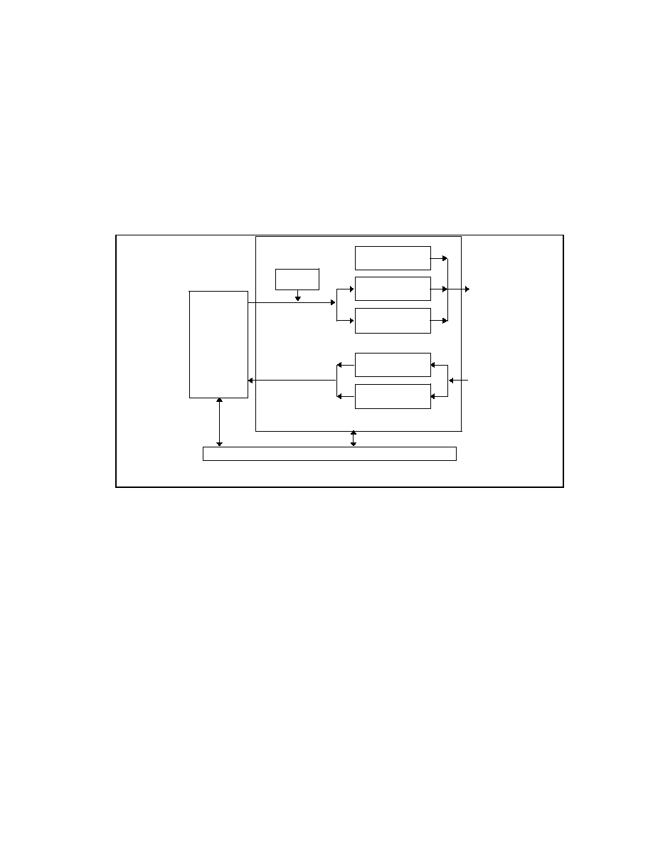
56
Consumer IR Mode
Transmit
nActiveFrame goes active as soon as the
Consumer IR transmitter starts modulating the
SCE data stream. nActiveFrame becomes
inactive as soon as the transmit register is
empty.
Receive
nActiveFrame goes active as soon as the
Consumer IR receiver detects the first active bit-
time of infrared energy. nActiveFrame becomes
inactive whenever the Consumer IR receiver is
manually disabled, a DMA Terminal Count has
occurred, or following a FIFO Overrun.
IRDA ENCODER
Description
The IrDA FIR Encoder supports the
synchronous bit-oriented HDLC protocol at
.576Mbps and 1.152Mbps, and 4PPM Encoding
at 4Mbps including all message framing, bit
stuffing, and CRC generation (Figure 21). The
IrDA FIR Encoder exchanges only payload data
with the host and supports Multi-Frame
Windows for brick walled messages as well as
BOF and BW framing extensions. The IrDA FIR
Encoder also includes an SIR Interaction Pulse
generator in hardware.
SCE
4PPM
Encoder
HDLC
Encoder
Tx
Rx
Framing
4PPM
Decoder
HDLC
Decoder
Control & Status
SIP
Generator
FIGURE 21 - IrDA FIR ENCODER
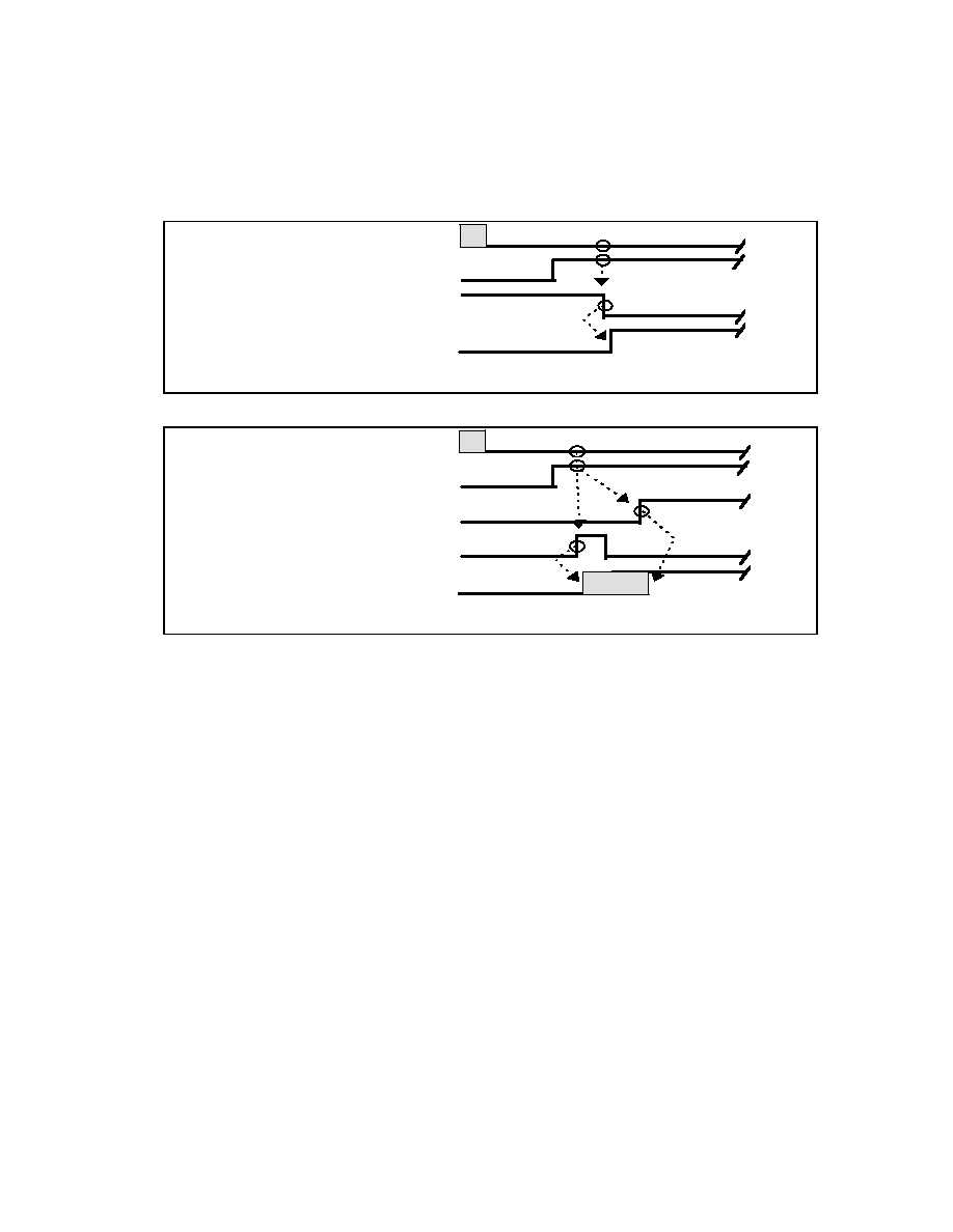
57
Transmit Timing
The SCE IrDA-mode transmitter is enabled by
setting the appropriate SCE MODES bits in SCE
Line Control Register B. If the FIFO Threshold
is zero, message transmission begins as soon
as transmit mode has been enabled and there is
data in the FIFO (Figure 22).
If the FIFO Threshold is greater than zero,
message transmission begins only after
transmit mode has been enabled and the FIFO
Threshold has been exceeded or TC is active
(Figure 23). NOTE: the IrDA-mode SCE
transmitter will only be enabled when the SIR
Interaction Pulse generator is inactive.
Once an IrDA transmission has begun, the End
of Message (EOM) and other state indicators
are cleared and the nActive Frame signal is
enabled. Following the frame check sequence,
EOM is reactivated and an EOM interrupt is
generated. Following the end of the frame,
nActive Frame is disabled (Figure 24).
F I F O E m p t y
T x E n a b l e
T r a n s m it
A c t i v e S I P T i m e
FIGURE 22 - IrDA FIR TRANSMIT ENABLE TIMING: FIFO THRESHOLD = 0
F I F O T h r e s h o l d
T x E n a b l e
T r a n s m it
T C
A c t iv e S I P T i m e
FIGURE 23 - IrDA FIR TRANSMIT TIMING: FIFO THRESHOLD > 0
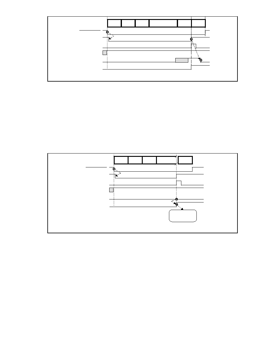
58
When active, the DATA DONE flag in Register
Block Zero, Line Control Register A alerts the
transmitter that the next FIFO underrun
condition signifies the end of the valid payload
data and that an EOF should begin (Figure 24).
During DMA operations TC automatically sets
the DATA DONE flag.
A message byte counter that is initialized with
the value in the data size register when the
message begins can also signal the end of the
valid payload data. If the message byte counter
goes to zero before the FIFO is empty and the
Brick Wall bit is one, a FIFO underrun with an
active DATA DONE flag is simulated, a
hardware CRC is appended (if required), and
the next message is brick walled (not shown).
If the FIFO is empty, the DATA DONE flag is
always cleared following the EOM, regardless of
how the bit was set. If the DATA DONE flag is
inactive when an underrun occurs, the
transmitter aborts the message and set the
Abort and Underrun errors appropriately (Figure
25).
EOF
FCS
I
C
A
BOF
EOM
EOM Interrupt
Tx Enable
Active Frame
Data Done
FIFO Empty
FIGURE 24 - IrDA FIR TX MESSAGE TIMING (SOFTWARE CRC)
I
C
A
BOF
EOM
EOM Interrupt
Tx Enable
Active Frame
Data Done/TC
FIFO Empty
Underrun Error
Abort Error
Abort
FIGURE 25 - TX ABORT ON UNDERRUN TIMING

59
Receive Timing
Once enabled using the SCE Modes bits in Line
Control Register B, the IrDA-mode receiver
begins searching for valid FIR frames. The
affects of non-valid IrDA infrared activity such
as out of spec pulse widths and invalid BOF
sequences are always reflected in the status
indicators in the IrCC registers. When a valid
BOF is detected, the EOM from the previous
message is disabled, errors are reset, and an
nActive Frame Interrupt is sent (Figure 26).
EOM and the EOM Interrupt are enabled
following an active FCS.
Framing errors or a FIFO overrun that occurs
before the Frame Check Sequence is complete
is indicated in the appropriate status register
bits and the message is aborted (Figure 27).
EOF
FCS
I
C
A
BOF
FIFO Empty
EOM Interrupt
Rx Enable
Active Frame
Active Frame Int.
EOM
FIGURE 26 - IrDA RX MESSAGE TIMING
I
C
A
BOF
FIFO Full
EOM Interrupt
Rx Enable
Active Frame
EOM
Active Frame Int.
Overrun Error
Abort Error
FIGURE 27 - IrDA FIR RX ABORT ON OVERRUN TIMING

60
CRC Select Timing
During transmit if the CRC Select control is low
the FCS is assumed to be part of the message
payload data sent from the Host and the
hardware CRC generator is not engaged (Figure
28). During receive if the CRC Select control is
low the hardware CRC generator is not
engaged, no comparison with the received FCS
is made, and the state of the configuration
register CRC Error flag is undefined.
During transmit if the CRC Select control is high
the FCS is assumed not to be part of the
message data sent from the Host, the hardware
CRC generator is engaged, and the FCS result
is appended to the Host payload data (Figure
29). During receive, if the CRC Select control is
high, the output from the hardware CRC
generator is compared to the CRC from the
received message and the result recorded in the
configuration register CRC Error flag. Note: for
all IrDA FIR received messages, the FCS is sent
to the Host through the FIFO regardless of the
state of the CRC Select control.
EOF
FCS
I
C
A
BOF
FIFO Empty
EOM
CRC Select
Data Done
TC
FIGURE 28 - IrDA FIR FRAME WITH SOFTWARE CRC
CRC
(HW)
EOF
FCS
I
C
A
BOF
FIFO Empty
EOM
CRC SELECT
Data Done
TC
FIGURE 29 - IrDA FIR FRAME WITH HARDWARE CRC

61
Framing Errors
The IrDA FIR pulse and signaling violations
listed in this section are considered framing
errors. When the Frame Error bit in the IrCC
Line Status register is one, a framing error has
occurred. The IrDA receiver response to
framing errors depends upon when the errors
occur. Framing errors that occur before a valid
BOF has been detected will always set the
Frame Error bit but will not alter the system
state in any other way; i.e., the abort bit is not
activated. If framing errors occur following a
valid BOF, i.e. while nActive Frame is zero, the
message is aborted. For both the HDLC and
4PPM encoding schemes, messages with data
fields larger than the value contained in the data
size register violate IrDA framing rules but are
not aborted. NOTE: the Size Error and the
Frame Error bits are set. Pulses less than 60ns
should be ignored, in all modes. The events
listed in the following two sections are framing
errors.
1.152Mbps
Pulse Widths greater than one bit-cell. Invalid
BOF: includes data fields before BOF, pulse-
width violations during BOF, and subsequent
invalid BOFs (including Aborts) following a valid
BOF before the Address field. Invalid data
fields: includes frames with invalid data field
characters (including aborts), and pulse-width
violations during a data field (including during
CRC). Invalid EOF fields: includes invalid EOF
flags (including Aborts), pulse-width violations,
and subsequent invalid EOFs following a valid
EOF.
4Mbps
Pulse Widths greater than two chip times.
Invalid PA field: includes invalid PA symbols,
pulse-width violations, and subsequent invalid
PA symbols following at least one valid PA
symbol (including Aborts) before the STA field.
Invalid STA field: includes invalid STA symbols,
pulse-width violations, and subsequent invalid
STA symbols following at least one valid symbol
(including Aborts) before the payload data.
Invalid Data field: includes frames with invalid
data symbols (including Aborts), and pulse-
width violations during a data field (including
during CRC). Invalid EOF field: includes invalid
EOF flag (including Aborts), pulse-width
violations, and subsequent invalid EOFs
following a valid EOF.
CONSUMER IR ENCODER TIMING
The Consumer IR-mode SCE does not require
the framing signals that are specified in the
IrDA-mode timing, although both modes utilize
the nActive Frame and EOM Interrupt. There is
also no need to differentiate the IrDA-mode
EOM signal from an inactive nActive Frame.
The Consumer IR-mode SCE operates at the bit
rates set in the Consumer IR Bit Rate Register.
The Consumer IR-mode SCE can operate in
Programmed I/O or DMA mode. The CRC
Generator is not used.
Transmit Timing
The SCE TV Remote transmitter uses the same
enabling mechanisms as the IrDA-mode
transmitter (see page 57). Note: the IrDA-mode
Active SIP Pulse Tx Enable timing restriction
does not apply. Once enabled, the TV Remote
transmitter operates until the FIFO underruns
(Figure 30). The nActive Frame and EOM
Interrupt signals behave as shown. The SCE
Modes bits are reset to zero, disabling the
transmitter, following nActive Frame.
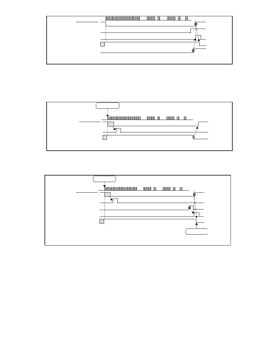
62
Receive Timing
The SCE TV Remote receiver can be enabled
with the configuration register SCE Modes bits,
polled using programmed I/O, and manually
disabled when sufficient data has been collected
(Figure 31). Once enabled, the SCE receiver will
only begin to interpret line data following the first
valid zero detection.
Figure 32 illustrates how the TV Remote
receiver operates using DMA. TC disables the
receiver, sends an EOM Interrupt, and resets
the SCE Modes bits to zero.
FIFO Empty
EOM Interrupt
Tx Enable
Active Frame
Tx Reg. Empty
FIGURE 30 - TV REMOTE TRANSMIT TIMING
Rx Enable
Active Frame
Active Frame Int.
Zero Detect
FIGURE 31 - TV REMOTE MANUAL RX TIMING
TC
EOM Interrupt
Rx Enable
Active Frame
Active Frame Int.
Zero Detect
Clear FIFO
FIGURE 32 - TV REMOTE DMA RX TIMING

63
The SCE TV Remote receiver will abort on a
FIFO Overrun condition. When the overrun
occurs the receiver is disabled, an EOM
Interrupt is sent, and the FIFO is flushed.
IRDA MULTI-FRAME WINDOW SUPPORT
The Tx Data Size register can be used with DMA
blocks that are larger than the size of an IrDA
message frame to support Multi-Frame
Windows, i.e. multiple unacknowledged
message frames. MFWs with a single DMA
block can occur in both Brick Walled and non-
Brick Walled modes.
Non-Brickwalled MFWs
To support non-Brick Walled multi-frame
windows set the SCE Modes bits to zero and
setup the DMA controller with a block-size larger
than a single frame but smaller-than or equal-to
the Tx Data Size
◊
8. Choose the appropriate
encoder, start the transmitter, and wait for an
EOM interrupt. Repeat this procedure by
reseting and then re-enabling the transmitter
DMA block-size
˜
Tx Data Size times, until the
DMA block has been transferred. Reset the
FIFO Threshold for the last frame, if necessary.
Brickwalled MFWs
To support Brick Walled Multi-Frame Windows
set the SCE Modes bits to zero and setup the
DMA controller with a block-size larger than a
single frame but smaller-than or equal-to the Tx
Data Size
◊
8. Choose the appropriate encoder,
initialize the Brick Wall Count, and set the Brick
Wall bit. Start the transmitter and wait for DMA
block-size
˜
Tx Data Size EOF interrupts or poll
the message count bits; i.e., until the DMA block
has been transferred.
LOOPBACK MODE
Loopback mode allows diagnostic testing of the
IrDA FIR and Consumer IR encoders.
Loopback tests require that the SCE FIFO be
used for both transmit and receive modes,
simultaneously. The Data Size registers are
used to constrain the Loopback test. Brick
Walled messages are not supported in
Loopback mode.
FIFO Full
EOM Interrupt
Rx Enable
Active Frame
Active Frame Int.
Zero Detect
Overrun
FIGURE 33 - TV REMOTE RX ABORT ON OVERRUN

64
Initialization
The FIFO must be loaded with the appropriate
transmit data while the Block Control bits in
SCE Configuration Register A are set to the
required transfer mode with the SCE MODES
bits set to Transmit/Receive Disabled. Enough
room must remain in the FIFO for receive data.
The Loopback Transmit CRC bit (D6) in SCE
Configuration Register B must be initialized for
the appropriate CRC response during loopback
testing. The Data Size registers must be
properly initialized to constrain the loopback
function so that received data is not re-
transmitted. The Rx Data Size register is
required for Consumer IR Loopback tests and
the Tx Data Size register is required for IrDA FIR
Loopback tests. The RX Data Size register
must be programmed with one less than the
total number of bytes in the CIR loopback test;
i.e., Test_byte_count_1. Proper programming of
the Tx Data Size register depends upon the
state of the CRC Select and Loopback Tx CRC
bits. The FIFO Threshold is not used for
loopback tests. The Tx Polarity and Rx Polarity
bits must be the same state for loopback tests.
Set the Loopback bit in SCE Configuration
Register B to begin the loopback test.
Retrieving Results
The loopback test data can be read from the
FIFO immediately following the End-of-
Message; i.e., the Loopback bit does not need to
be reset, nor does the FIFO need to be explicitly
re-configured for ISA bus access.
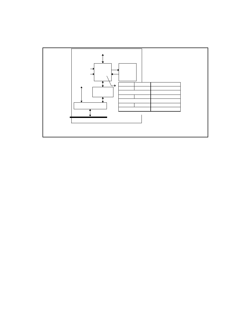
65
BUS INTERFACE I/O
The Bus Interface I/O block contains a 128-byte
FIFO, DMA/Interrupt logic, and multiplexers to
control access to the FIFO and the ISA Bus
(Figure 34).
The Databus Multiplexer provides exclusive ISA
Bus access to either the 16550A UART or the
IrCC SCE depending on the state of Block Mode
Controls in the configuration registers. Disabled
blocks are tristated from the ISA Bus.
FIFO MULTIPLEXER
SCE FIFO Access
The FIFO Multiplexer controls the configuration
of the SCE FIFO in the Bus Interface I/O Block.
This configuration can be inferred from the state
of the SCE Modes bits in Line Control Register
B: when the transmit/receive modes are
disabled, or the transmit mode is enabled, the
FIFO is configured for transmit; otherwise, the
FIFO is configured for receive. The signal
Transmit in Figure 34, above, can be satisfied
by the inverse of the SCE Modes msb; e.g.,
nD7.
HOST FIFO Access
The Host always has read access to the FIFO,
regardless of the state of the SCE Modes bits,
or the Loopback bit. The Host has write access
to the FIFO when the Loopback bit is inactive
and the transmit/receive modes are disabled or
the Transmit mode is enabled.
128-BYTE SCE FIFO
FIFO Timing & Controls
The FIFO uses interleaved access timing to
allow simultaneous FIFO data reads and data
FIFO
Multiplexer
128-byte
FIFO
Transmit
Loopback
SCE
Databus Multiplexer
16550A UART
ISA Bus
Loopback
Transmit
Function
0
0
FIFO In to SCE Rx
FIFO Out to Host Bus
0
1
FIFO In to Host Bus
FIFO Out to SCE Tx
1
X
FIFO In to SCE Rx
FIFO Out to SCE Tx
I/O & Interrupt
Control
FIGURE 34 - BUS INTERFACE I/O BLOCK

66
writes. This is required both for normal
operation with asynchronous Host/ SCE access
timing, and during loopback tests with
synchronous SCE-only access timing where the
FIFO is simultaneouly used for transmit and
receive. FIFO controls include, separate read/
write lines, FIFO Full and FIFO Not Empty flags,
Reset, FIFO Threshold, and Interrupt.
FIFO Threshold
Description
The SCE FIFO Threshold generates
programmed I/O service requests to
accommodate systems with widely varying I/O
response times. FIFO Threshold values
typically reflect the overall I/O response
characteristics of a system. The same
threshold value can be used for both I/O read
and I/O write cases. During DMA operatons, the
FIFO Threshold is only used to trigger the SCE
transmitter.
The FIFO Threshold value is programmable
from 0 to 127. The FIFO Threshold Register,
located in Register Block One, Address Two,
contains the FIFO Threshold value. Low
threshold values result in longer periods of time
between service requests because more of the
FIFO is utilized before the request is issued.
Systems that program low threshold values
must typically provide fast response times to
these requests; i.e., high performance systems
that move I/O data quickly.
High threshold values are used in "sluggish"
systems with long service request latencies.
Low performance systems typically take longer
to move I/O data and require more frequent I/O
service. For systems that program high FIFO
threshold values, much less of the FIFO is
utilized before service requests are issued.
Receive Threshold
Once the FIFO Interrupt is enabled, Receive
Service Requests (RxServReq), i.e. data
transfers from the FIFO to the host, are
generated whenever there are 128 minus the
FIFO Threshold value or more data bytes in the
FIFO, given by:
RxServReq
128 - FIFO Threshold
For example, if the FIFO Threshold value is 12,
RxServReq will be active whenever there 116 to
128 data bytes in the FIFO. If the FIFO
Threshold is 0, RxServReq will be active
whenever the FIFO is full. If the FIFO Threshold
is 127, RxServReq will be active whenever the
FIFO is not empty.
Transmit Threshold
Once the FIFO Interrupt is enabled, Transmit
Service Requests (TxServReq), i.e. data
transfers from the host to the FIFO, are
generated whenever there are FIFO Threshold
value or fewer data bytes in the FIFO, given by:
TxServReq
FIFO Threshold
For example, if the FIFO Threshold value is 12,
TxServReq will be active whenever there are 12
or less data bytes in the FIFO. If the FIFO
Threshold is 0, TxServReq will be active
whenever the FIFO is empty. If the FIFO
Threshold value is 127, TxServReq will be active
whenever the FIFO is not full.
FIFO Interrupt
The FIFO Interrupt becomes active whenever
the FIFO Interrupt Enable is active and either
TxServReq or RxServReq is active. When FIFO
Interrupt Enable becomes inactive, the FIFO
Interrupt goes inactive.
For example, the FIFO Interrupt will become
active during a transmit operation if the FIFO
Threshold is fifty, the FIFO Interrupt Enable is
active, and there are from one to fifty data bytes
in the FIFO (Figure 35).
In Figure 35, notice that five bytes are written to
the FIFO every time a service request is
answered. The third request occurs as soon as

67
the FIFO Interrupt Enable is activated because
the five bytes written to the FIFO following the
second service request was not enough data to
exceed the FIFO Threshold given the long
interrupt latency.
DMA
The DMA channel works in Single-Byte and
Burst (Demand) Mode. AEN is high during DMA
transfers. The DMA controls are located in SCE
Configuration Register B. When the DMA
Enable bit (D0) is one, DMA is enabled. The
DMA Burst Mode bit (D1) controls the DMA
mode. DRQ is further gated by the SCE Modes
bits; e.g., DRQ can only be enabled if either
Transmit or Receive mode has been enabled.
During transmit DRQ remains active as long as
the FIFO is not full until TC. During receive
DRQ remains active as long as the FIFO is not
empty until TC.
Single-Byte Mode
Single-Byte mode is enabled by resetting the
DMA Burst bit in SCE Configuration Register B.
Single-Byte DMA transfers one data byte for
each DRQ (Figure 36). Terminal Count occurs
only once, during the last byte of data block.
FIFO Int. Enable
FIFO Interrupt
Service Req.
Satisfied
Data Bytes in
FIFO 51
50
49
54
...
51
50
49
48
47
46
45
44
49
48
...
Serv. Req. Satisfied
(long int. latency)
1st Service
Request
2nd Service
Request
3rd Service
Request
TxServReq
FIGURE 35 - FIFO INTERRUPT EXAMPLE
DMA Enable
DRQ
I/Ox
nDACK
DMA Burst
AEN
TC
FIGURE 36 - DMA SINGLE-BYTE MODE TIMING
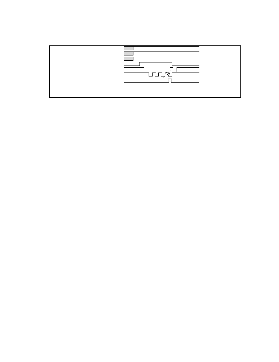
68
Burst (Demand) Mode
DMA Burst mode is enabled by setting the DMA
Burst bit in SCE Configuration Register B.
Demand Mode DMA transfers up to 32 data
bytes for each DRQ (Figure 37). The IrCC
guarantees that DRQ relinquishes the ISA bus
after thirty-two DMA I/O read or write cycles to
allow for memory refresh.
32 I/Ox Clock DMA Refresh Counter
The 32 I/Ox Clock DMA Refresh Counter is used
to prevent DRQ from staying active for more
than 32 I/O read/write cycles at a time.
The counter is stopped and preloaded whenever
DRQ is not active. Once DRQ becomes active,
the counter decrements until zero-count or DRQ
is deactived.
In Demand Mode, the count-zero condition
always clears DRQ and triggers a Refresh
Interval. The Refresh Interval remains active for
350ns following an inactive nDACK (Figure 38).
If there is more data to transfer, DRQ goes
active again and the cycle repeats.
Single Byte Mode DMA does not use the 32 I/Ox
Clock Refresh Counter.
D M A E n a b l e
D R Q
I / O x
n D A C K
D M A B u r s t
A E N
T C
FIGURE 37 - DMA BURST MODE TIMING

69
Burst Mode Transmit
Uses FIFO Threshold for Triggered Transmit.
The IrDA 4PPM transmit encoder can deplete
the SCE FIFO faster than an ISA Host can fill it.
The FIFO Threshold can be used to allow the
DMA controller to load enough data into the
FIFO before transmission begins to
accommodate system latencies for subsequent
DMA transfer cycles. The FIFO Threshold is
otherwise not used for DMA transfers.
DRQ Control
In DMA Burst Mode, DRQ remains active until
the entire DMA data block has been transferred,
as indicated by DMA Terminal Count (TC). The
internal FIFO Full signal can temporarily
deactivate DRQ if the DMA block has not been
completely transferred but there is no room left
in the FIFO for more data. As soon as the FIFO
Full becomes inactive, DRQ is reasserted. The
internal Refresh Interval signal can also
temporarily deactivate DRQ (see the 32 I/Ox
Clock DMA Refresh Counter).
Example: Transmit a 256-Byte IrDA Message
1. Setup and enable the DMA controller for the
256-byte message.
2. Set the appropriate FIFO Threshold,
typically this number can be high, e.g. 127,
and set the SCE Modes bits in Register
Block Zero, Address 6 to enable the
transmitter.
3. The DMA controller proceeds to load the
FIFO until TxServReq activates the
transmitter. DMA transfer cycles continue
until TC. DRQ is only de-asserted when
FIFO Full or Refresh Interval are active
(Figure 39).
DMA Enable
DRQ
I/Ox
nDACK
Refresh Interval
32 clocks
max.
350ns
min.
Disable 32-Clk
Countdown & Reset
32-Clk Counter
Enable 32-Clk
Countdown
DMA Burst
FIGURE 38 - 32 I/OX CLOCK DMA REFRESH COUNT TIMING
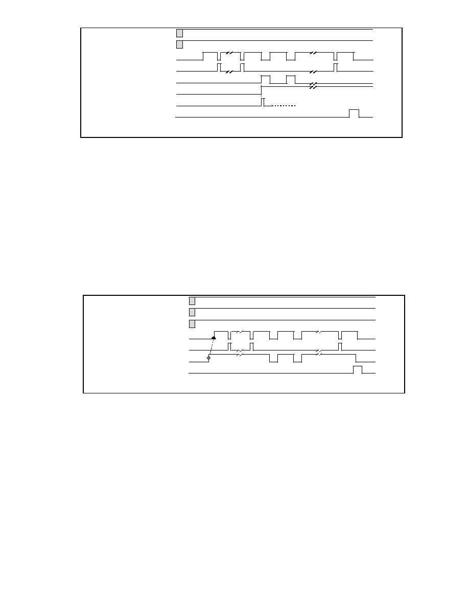
70
Burst Mode Receive
DRQ Control
In DMA Burst Mode, DRQ remains active until
the entire DMA data block has been transferred,
as indicated by DMA Terminal Count (TC).
Since the FIFO Threshold is not used for DMA
transfer cycles, DRQ is asserted as soon as
FIFO Not Empty is true. FIFO Not Empty can
temporarily deactivate DRQ if the DMA block
has not been completely transferred but there is
no data left in the FIFO to transfer. As soon as
FIFO Not Empty becomes true, DRQ is
reasserted. The internal Refresh Interval signal
can also temporarily deactivate DRQ (see the
32 I/Ox Clock DMA Refresh Counter).
Example: Receive a 256-Byte IrDA Message
1. Setup and enable the DMA controller for the
256-byte message.
2. Enable the IrDA Receiver.
3. DRQ is asserted as soon as FIFO Not
Empty is true.
4. The DMA controller proceeds to empty the
FIFO until TC. DRQ is otherwise only de-
asserted when FIFO Not Empty is false or
Refresh Interval is active (Figure 40).
D M A E n a b l e
D R Q
T C
F I F O F U L L
D M A B u r s t
R e f r e s h I n t e r v a l
T x E n a b l e
T x S e r v R e q
FIGURE 39 - DMA BURST MODE TRANSMIT TIMING
D M A E n a b l e
D R Q
T C
F I F O N O T E M P T Y
D M A B u r s t
R e f r e s h I n t e r v a l
R x E n a b l e
FIGURE 40 - DMA BURST MODE RECEIVE TIMING

71
PROGRAMMED I/O
Programmed I/O mode is selected when the
DMA Enable bit in SCE Configuration Register B
is zero.
The IrCC also supports String Move timing
which is a block-mode programmed I/O
operation that utilizes IOCHRDY to control the
transfer (Figure 41). String Move mode is
selected when the String Move bit in SCE
Configuration Register B is one.
Polling Interface
Programmed I/O without IOCHRDY requires
polling the FIFO status flags before reading or
writing FIFO data. The Receiver interface
depends upon the FIFO Not Empty flag. If FIFO
Not Empty is true, there is read data available in
the FIFO (Figure 42). The Transmitter interface
depends upon the FIFO Full flag. If FIFO Full is
false, there is room for write data in the FIFO (
Figure 43).
F I F O N o t E m p t y
I O C H R D Y
I O R
String M o v e
A E N
FIGURE 41 - STRING MOVE TIMING
DMA Enable
IOR
String Move
FIFO Data READ
Status READ
FIFO NOT EMPTY
FIGURE 42 - PROGRAMMED I/O READ TIMING
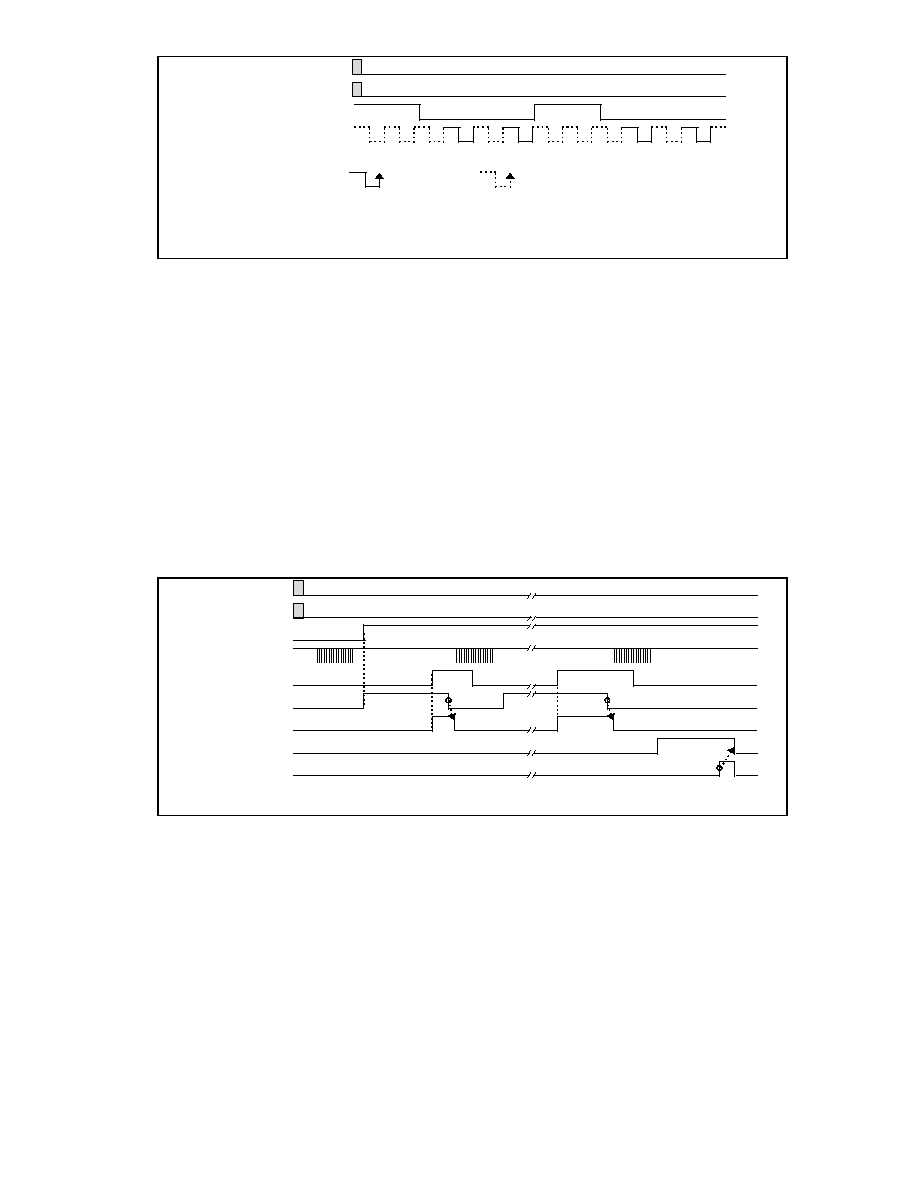
72
FIFO Interrupt Interface
Transmit
Description
Transmitting messages with Programmed I/O
using FIFO Interrupt requires writing a fixed
number of data bytes, usually related to the
threshold, whenever the FIFO Interrupt becomes
active. An appropriate FIFO Threshold value
allows the host to efficiently satsify the FIFO
service requests until the message transmission
is complete. For slow systems, the FIFO can be
manually filled with transmit data before the
transmitter is enabled. Note: the FIFO will
automatically request service before the
transmitter is activated if the FIFO Threshold is
greater than zero.
Example: Transmit a 256-byte IrDA Message
1. Set an appropriate FIFO Threshold for the
system type. For the greatest performance
advantage, pre-load the FIFO with transmit
data.
2. Set the FIFO Interrupt Enable active and
activate the transmitter.
3. Service the FIFO Interrupts as required.
Set the Data Done flag when all of the
transmit message data has been loaded
(Figure 44).
DMA Enable
IOW
String Move
FIFO Data WRITE
Status READ
FIFO FULL
FIGURE 43 - PROGRAMMED I/O WRITE TIMING
DMA Enable
IOW
String Move
Tx Enable
TxServReq
FIFO Int. Enable
FIFO Interrupt
Data Done
EOM Interrupt
FIGURE 44 - INTERRUPT DRIVEN PROGRAMMED I/O TRANSMIT TIMING

73
Receive
Description
Receiving messages with Programmed I/O
using FIFO Interrupt requires reading a fixed
number of data bytes, usually related to the
threshold, whenever the FIFO Interrupt becomes
active. An appropriate FIFO Threshold value
allows the host to efficiently satisfy the FIFO
service requests until the message reception is
complete.
Example: Receive a 256-byte IrDA Message
1. Set an appropriate FIFO Threshold for the
system type.
2. Set the FIFO Interrupt Enable active and
enable the receiver.
3. Service the FIFO Interrupts as required
(Figure 45). Note: the amount of data
remaining in the FIFO following the last
service request (RxServReq) in Figure 45 is
probably less than the typical read block
size. This will occur when an IrDA EOF has
been detected, the FIFO Receive Threshold
has not been reached and the FIFO Not
Empty flag is true.
IOCHRDY Time-out
Description
In programmed I/O mode when AEN = low and
String Move = active, IOCHRDY can be used to
slightly extend the access cycle if the FIFO is
temporarily unable to fulfill the transfer request
(Figure 46). If IOCHRDY remains inactive for
more than 10us, a time-out error occurs and
subsequent IOCHRDY cycles are prevented
until the string move bit is specifically
reactivated. Because of the 10us IOCHRDY
time-out, it is recommended that string move
timing only be used for 1.152Mbps transfers and
above.
DMA Enable
IOR
String Move
Rx Enable
RxServReq
FIFO Int. Enable
FIFO Interrupt
EOM Interrupt
FIGURE 45 - INTERRUPT DRIVEN PROGRAMMED I/O RECEIVE TIMING

74
IOCHRDY Timer
The 10us IOCHRDY Timer is initialized when
IOCHRDY is active. The timer count sequence
is activated when IOCHRDY goes inactive. If
IOCHRDY becomes active before the 10us time-
out has elapsed, the timer is stopped and the
count is re-initialized. If IOCHRDY is still
inactive when the 10us time-out occurs, the
timer stops, the time-out error bit is set,
IOCHRDY is re-asserted, and the string move
bit is reset (Figure 47).
String Move
IOCHRDY
IOR
FIFO Not Empty
AEN
24ns (max)
10us (max)
FIGURE 46 - VALID I/O READ READY CYCLE
String Move
IOCHRDY
IOR
FIFO Not Empty
AEN
10us
IOCHRDY Time-out
Start
Timer
IOCHRDY
Error
FIGURE 47 - IOCHRDY 10uS TIME-OUT
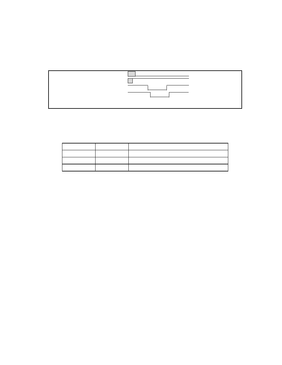
75
Zero Wait State Support
nSRDY
nSRDY can be driven by the IrCC to indicate
that an access cycle shorter than the standard
I/O cycle can be executed. NOTE: the names
nSRDY & nNOWS can be used interchangeably.
nSRDY is enabled by the No Wait bit in SCE
Configuration Register B. When No Wait is
one, nSRDY goes active following the trailing
edge of the ISA I/O command and inactive
following the rising edge (Figure 48). nSRDY is
suppressed during DMA & refresh cycles, i.e.
when AEN is active, or when IOCHRDY is
inactive. Zero Wait State support is only
available when the SCE is enabled.
The Interaction of nSRDY and IOCHRDY
nSRDY and IOCHRDY determine the three
types of ISA access cycles: no-wait-state cycle,
standard cycle, ready cycle (Table 32). NOTE:
An inactive IOCHRDY suppresses nSRDY.
Table 32 - nSRDY and IOCHRDY Interaction
nSRDY
IOCHRDY
DESCRIPTION
active
active
No-wait-state Cycle (shortest length)
inactive
active
Standard Cycle (mean length)
x
inactive
Ready Cycle (longest length)
AEN
I/Ox
nSRDY
No Wait
FIGURE 48 - nSRDY TIMING
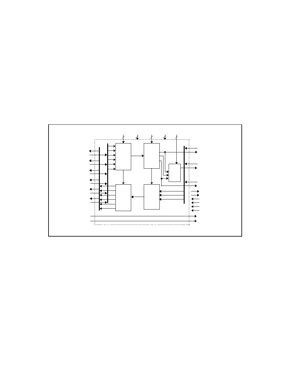
76
OUTPUT MULTIPLEXER
The Output Multiplexer routes the active
encoder/decoder to one of three IrCC serial
communications ports. There are no restrictions
on any of these connections other than Rx/Tx
source pairs go to the same destination (Figure
49). Descriptions of the Block Control, Output
Mux. and Aux IR signals can be found in the
SCE Configuration Registers in Register Block
One.
There are Rx and Tx Polarity controls that
determine the active states for the IR port
signals, see SCE Configuration Register A. The
state of inactive IR outputs depends upon the
Tx Polarity bit; e.g., if Tx Polarity is zero
(default), inactive outputs will be one. Routing
for the COM Port flow-control signals is fixed.
When the COM Port is inactive, the flow-control
signals behave according to the current SMSC
16550A serial port specification. The Tx/Rx
Polarity bits do not apply when COM mode is
selected. There is a provision for added
transmit current capacity by selectively
duplicating the transmit output of the IR Port or
the COM Port at the AUX Port. This can be
used, for example, to accommodate the high-
power optics found in Consumer IR TV remote
controls.
There are GP Data pins that always reflects the
state of General Purpose Data & Fast bits (5-6)
of Line Control Register A, in Register Block
Zero, Address Four. The state of the G.P. Data
pins is independent of the IrCC Block Controls
or the Output Multiplexer.
IRRx
IRTx
ARx
ATx
CRx
CTx
nDSR
nRTS
nDTR
nCTS
nDCD
nRI
1 to 3
Demux.
3 to 1
Mux.
1 to 6
Demux.
6 to 1
Mux.
2 to 1
Mux.
Raw Rx
Raw Tx
TV Rx
TV Tx
ASK Rx
ASK Tx
IrDA SIR Rx
IrDA SIR Tx
COM Rx
COM Tx
Output
Mux.
2
4
Block
Control
Aux.
IR
1
IR
Port
AUX
Port
COM
Port
1
Tx
Polarity
1
Rx
Polarity
G.P. Data
GP Data G.P.
Port
IrDA FIR Rx
IrDA FIR Tx
Fast
Fast
FIGURE 49 - OUTPUT MULTIPLEXER BLOCK
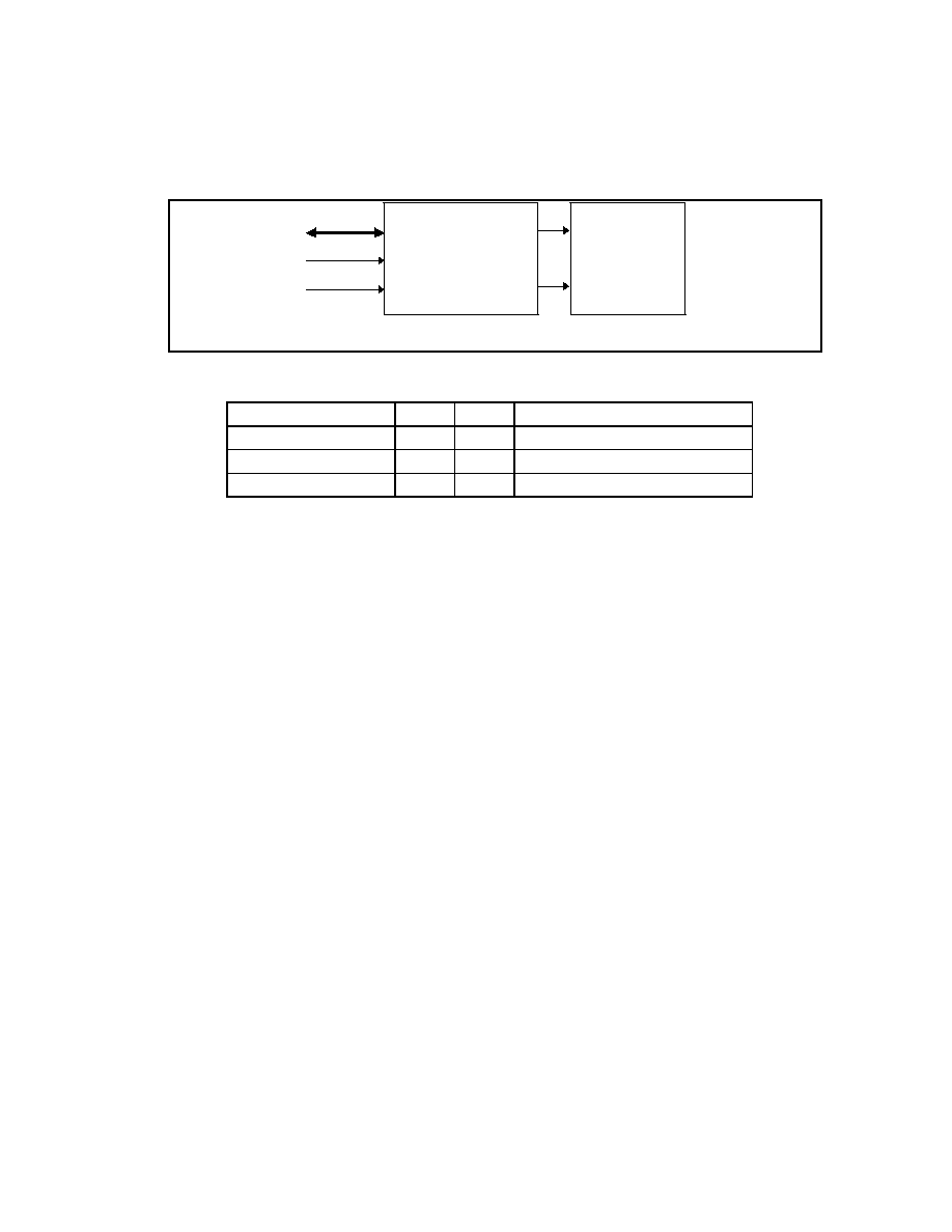
77
CHIP-LEVEL IrCC ADDRESSING SUPPORT
IrCC Register addressing is controlled at the
chip level. Both the ACE bank select, nACE,
and the SCE bank select, nSCE, are decoded at
the chip level from the Host Address Bus to
access data in the IrCC register banks (Figure
50). Table 33 illustrates a chip-level IrCC
address decoder using a base address of 2F8
for the ACE UART and 2F8+400 or 6F8 for the
SCE registers.
Table 33 - IrCC Address Decode at '400'hex
HEX ADDRESS
NACE
NSCE
DESCRIPTION
2F8 - 2FF
0
1
ACE UART registers enabled
6F8 - 6FF
1
0
SCE registers enabled
All other registers
1
1
IrCC registers not accessible
Chip-Level
Address
Decoder
ACE
Select
SCE
Select
Address Bus
AEN
I/O Select
nACE
nSCE
IrCC
FIGURE 50 - CHIP-LEVEL IrCC ADDRESS DECODE
78
AC TIMING
IR RX PULSE REJECTION
ENCODER
PULSE REJECTION
4PPM
72.8ns
HDLC 1.152Mbps
72.8ns
HDLC .576Mbps
145.6ns
IrDA SIR
60.0ns
Consumer IR
166ns
IRDA 4PPM
Bit Rate Tolerance
TBD of Bit Rate
Rx Pulse Width
MIN.
NOM.
MAX.
Single Pulse
85ns
125ns
TBD
Double Pulse
210ns
250ns
290ns
IRDA HDLC
Bit Rate Tolerance
TBD of Bit Rate Max
Rx Pulse Width
MIN.
NOM.
MAX.
.576Mbps
TBD
434ns
TBD
1.152Mbps
TBD
217ns
TBD

79

1996© STANDARD MICROSYSTEMS CORP.
Circuit diagrams utilizing SMSC products are included as a means of illustrating
typical applications; consequently complete information sufficient for construction
purposes is not necessarily given. The information has been carefully checked
and is believed to be entirely reliable. However, no responsibility is assumed for
inaccuracies. Furthermore, such information does not convey to the purchaser of
the semiconductor devices described any licenses under the patent rights of
SMSC or others. SMSC reserves the right to make changes at any time in order to
improve design and supply the best product possible. SMSC products are not
designed, intended, authorized or warranted for use in any life support or other
application where product failure could cause or contribute to personal injury or
severe property damage. Any and all such uses without prior written approval of
an Officer of SMSC and further testing and/or modification will be fully at the risk of
the customer.
IrCC Rev. 5/10/96