 | –≠–ª–µ–∫—Ç—Ä–æ–Ω–Ω—ã–π –∫–æ–º–ø–æ–Ω–µ–Ω—Ç: CXA1685M | –°–∫–∞—á–∞—Ç—å:  PDF PDF  ZIP ZIP |
High-Speed Transimpedance Amplifier
Description
CXA1685M is a low noise transimpedance
amplifier, particularly suitable for fiber-optic system.
CXA1685M is fabricated using high-speed bipolar
process.
Features
∑ High transimpedance:
Q 11.2k
(Typ.)
Q 10.8k
(Typ.)
∑ Wide band width (≠3dB): Q 177MHz (Typ.)
Q 157MHz (Typ.)
∑ Maximum input current:
1mA
∑ Low noise:
1.7pA/
Hz (Typ.)
Applications
∑ SONET/SDH: 155Mb/s
∑ Fiber channel: 133Mb/s
∑ FDDI:
125Mb/s
Absolute Maximum Ratings
∑ Supply voltage
V
CC
≠ V
EE
≠0.3 to +7.0 V
∑ Minimum input voltage V
IN
V
EE
V
∑ Input current
I
IN
≠1 to +1 mA
∑ Output current
(Q/Q)
(Continuous)
I
O
0 to 50
mA
(Surge)
0 to 100 mA
∑ Storage temperature
Tstg
≠65 to +150 ∞C
Recommended Operating Conditions
∑ DC power supply voltage
V
CC
≠ V
EE
4.75 to 5.46 V
∑ Operating ambient temperature
Ta
0 to +85
∞C
Structure
Bipolar silicon monolithic IC
≠ 1 ≠
E94X22A8Y
Sony reserves the right to change products and specifications without prior notice. This information does not convey any license by
any implication or otherwise under any patents or other right. Application circuits shown, if any, are typical examples illustrating the
operation of the devices. Sony cannot assume responsibility for any problems arising out of the use of these circuits.
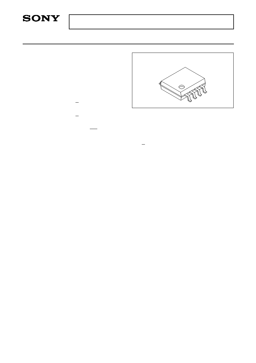
CXA1685M
8 pin SOP (Plastic)
≠ 2 ≠
CXA1685M
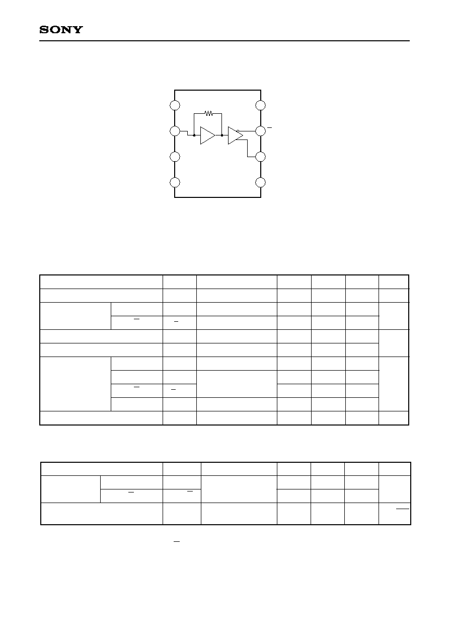
Block Diagram and Pin Assignment
∑ AC Electrical Characteristics
(V
CC
= V
CC
A = GND, V
EE
S = V
EE
DA = ≠5.46 to ≠4.75V, Ta = 0 to +85∞C)
Item
Symbol
Test Condition
Min.
Typ.
Max.
Unit.
Bandwidth
(≠3dB)
Input Current Noise Spectral
Density (Mean value)
Q
Q
f≠3dBQ
f≠3dBQ
1
In
fN = 1kH
Z
to 156MH
Z
113
109
177
157
1.7
MH
Z
pA/
HZ
1
Assumes photodiode capacitance; C
PD
< 1.0pF, output load capacitance; Cout = 2.0pF,
output load resistor; Q: 620
to V
EE
, Q: 1.3k
to V
EE
4
5
7
8
1
2
3
6
Z
T
V
CC
A
V
CC
Q
IN
Q
C
V
EE
DA
V
EE
S
Electrical Characteristics
∑ DC Electrical Characteristics
(V
CC
= V
CC
A = GND, V
EE
S = V
EE
DA = ≠5.46 to ≠4.75V, Ta = 0 to +85∞C)
Item
Symbol
Test Condition
Min.
Max.
Typ.
Unit
Supply current
Transimpedance
Max. Input Current before clipping
Max. Input Current
Bias votlage
I
EE
Z
TQ
Z
TQ
I
IN
I
IN2
V
IN
V
Q
V
Q
V
C
C
IN
input pin left open
Q
Q
IN
Q
Q
C
input pin left open
≠15.3
6.6
6.2
+40
+1000
≠10.0
11.2
10.8
V
EE
+ 2.5
V
EE
+ 1.7
V
CC
≠ 2.4
V
EE
+ 1.7
1.3
14.8
14.3
Ta = 25∞C
Input capacitance
mA
k
µA
V
pF

≠ 3 ≠
CXA1685M
Application Circuit
Application circuits shown are typical examples illustrating the operation of the devices. Sony cannot assume responsibility for
any problems arising out of the use of these circuits or for any infringement of third party patent and other right due to same.
Cautions for Handling
1. As the electronic breakdown level is weak, take care to handle.
2. The internal resistor of the output pin does not have the capability of drive (R
L
= 10k
). The terminal
resistors must be connected. The resistance value is shown in application circuit.
V
CC
A
V
CC
IN
Q
C
V
EE
DA
V
EE
S
4
5
7
8
1
2
3
6
Z
T
Q
V
CC
V
EE
1.0µF
0.1µF
0.1µF
620
1.3k
PD
Q
Q

≠ 4 ≠
CXA1685M
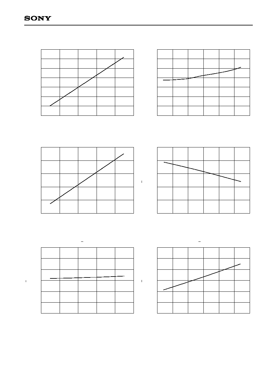
Typical Performance
Typical frequency characteristics (V
CC
≠ V
EE
= 5.0V, Ta = 25∞C)
Typical Output Wave forms (V
CC
≠ V
EE
= 5.0V, Ta = 25∞C)
f≠3dB = 157MHz
Q Output
5dB/div
0
500M
1.0G
65.9000ns
90.9000ns
115.900ns
V
IN
= ≠36dBm, f
IN
= 80MHz
20mV/div
Q
Q
Duty Cycle Distortion vs Input Current
f≠3dB = 177MHz
Q Output
5dB/div
0
500M
1.0G
Q Output
f
IN
= 155Mbps
55
50
45
40
35
30
0
200
400
600
800
1000
I
IN
[µA]
Q
O
u
t
p
u
t
D
C
D
[
%
]
Q Output
I
IN
[µA]
f
IN
= 155Mbps
55
50
45
40
35
30
0
200
400
600
800
1000
Q
O
u
t
p
u
t
D
C
D
[
%
]

≠ 5 ≠
CXA1685M
V
Q
vs I
IN
140
150
160
170
180
190
200
f≠3dBQ vs V
EE
Ta = ≠40∞C
Ta = 25∞C
Ta = 85∞C
140
150
160
170
180
190
200
f≠3dBQ vs Ta
V
CC
≠ V
EE
= 5.0V
V
CC
≠ V
EE
= 5.5V
140
150
160
170
180
190
200
f≠3dBQ vs Ta
V
CC
≠ V
EE
= 4.7V
V
CC
≠ V
EE
= 5.0V
V
CC
≠ V
EE
= 5.5V
140
150
160
170
180
190
200
f≠3dBQ vs V
CC
≠V
EE
Ta = ≠40∞C
Ta = 25∞C
Ta = 85∞C
f
≠
3
d
B
[
M
H
z
]
f
≠
3
d
B
[
M
H
z
]
V
Q
[
V
]
≠4.5
≠1
≠1.5
≠2
≠2.5
≠3
≠3.5
≠4
V
Q
vs I
IN
Ta = 85∞C
Ta = 25∞C
Ta = ≠40∞C
f
≠
3
d
B
[
M
H
z
]
f
≠
3
d
B
[
M
H
z
]
≠4.5
≠1
≠1.5
≠2
≠2.5
≠3
≠3.5
≠4
≠4.6
V
EE
[V]
≠5.6
≠5.4
≠5.2
≠5.0
≠4.8
100
Ta [∞C]
≠50
≠25
0
25
50
75
100
Ta [∞C]
≠50
≠25
0
25
50
75
≠4.6
V
EE
[V]
≠5.6
≠5.4
≠5.2
≠5.0
≠4.8
I
IN
[µA]
0
200
50
100
150
200
I
IN
[µA]
0
50
100
150
Ta = 85∞C
Ta = 27∞C
Ta = ≠40∞C
V
CC
≠ V
EE
= 4.7V
©
V
Q
[
V
]
≠ 6 ≠
CXA1685M
100
100
≠4.6
≠10.2
≠8.8
≠10
≠9.8
≠9.6
≠9.4
≠9.2
≠9
I
EE
vs V
EE
V
EE
[V]
≠5.6
≠5.4
≠5.2
≠5
≠4.8
Ta = 25∞C
V
EE
[V]
≠4
≠3
≠3.8
≠3.6
≠3.4
≠3.2
V
Q
vs V
EE
≠5.6
≠5.4
≠5.2
≠5
≠4.8
Ta = 25∞C
≠4.6
I
E
E
[
m
A
]
V
Q
[
V
]
≠4.6
≠3
≠1.8
≠2.8
≠2.6
≠2.4
≠2
V
Q
vs V
EE
V
EE
[V]
≠5.6
≠5.4
≠5.2
≠5
≠4.8
Ta = 25∞C
≠2.2
100
Ta [∞C]
V
Q
vs Ta
≠50
≠25
25
50
75
V
EE
= ≠5.0V
0
Ta [∞C]
≠10.2
≠8.8
≠10
≠9.8
≠9.6
≠9.4
≠9.2
≠9
I
EE
vs Ta
≠50
≠25
25
50
75
V
EE
= ≠5.0V
0
≠50
≠4
≠3
≠3.8
≠3.6
≠3.4
≠3.2
V
Q
vs Ta
Ta [∞C]
≠25
25
50
75
V
EE
= ≠5.0V
0
≠3
≠1.8
≠2.8
≠2.6
≠2.4
≠2
I
E
E
[
m
A
]
≠2.2
V
Q
[
V
]
V
Q
[
V
]
V
Q
[
V
]
≠ 7 ≠
CXA1685M
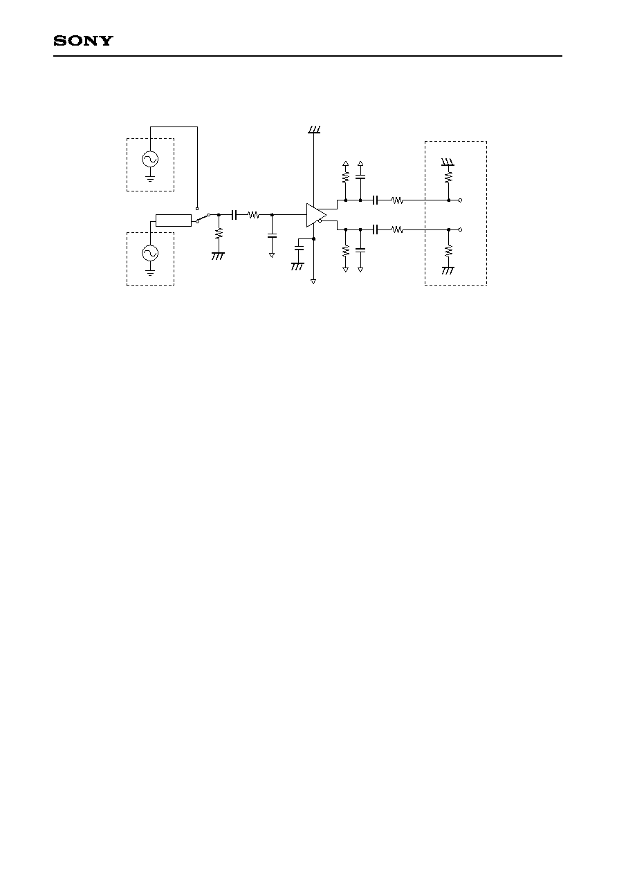
Test Circuit (Ta = 25∞C, V
EE
= ≠5.0V)
≠40dB
ATT
100
1µ
2p
1.3k
2p
51
0.1µ
51
0.1µ
2p
620
50
50
Signal Generator
Tracking Generator
Spectrum Analyzer/
Oscilloscope
51
680p
V
EE
V
EE
V
EE
V
EE
V
EE
V
EE
≠ 8 ≠
CXA1685M
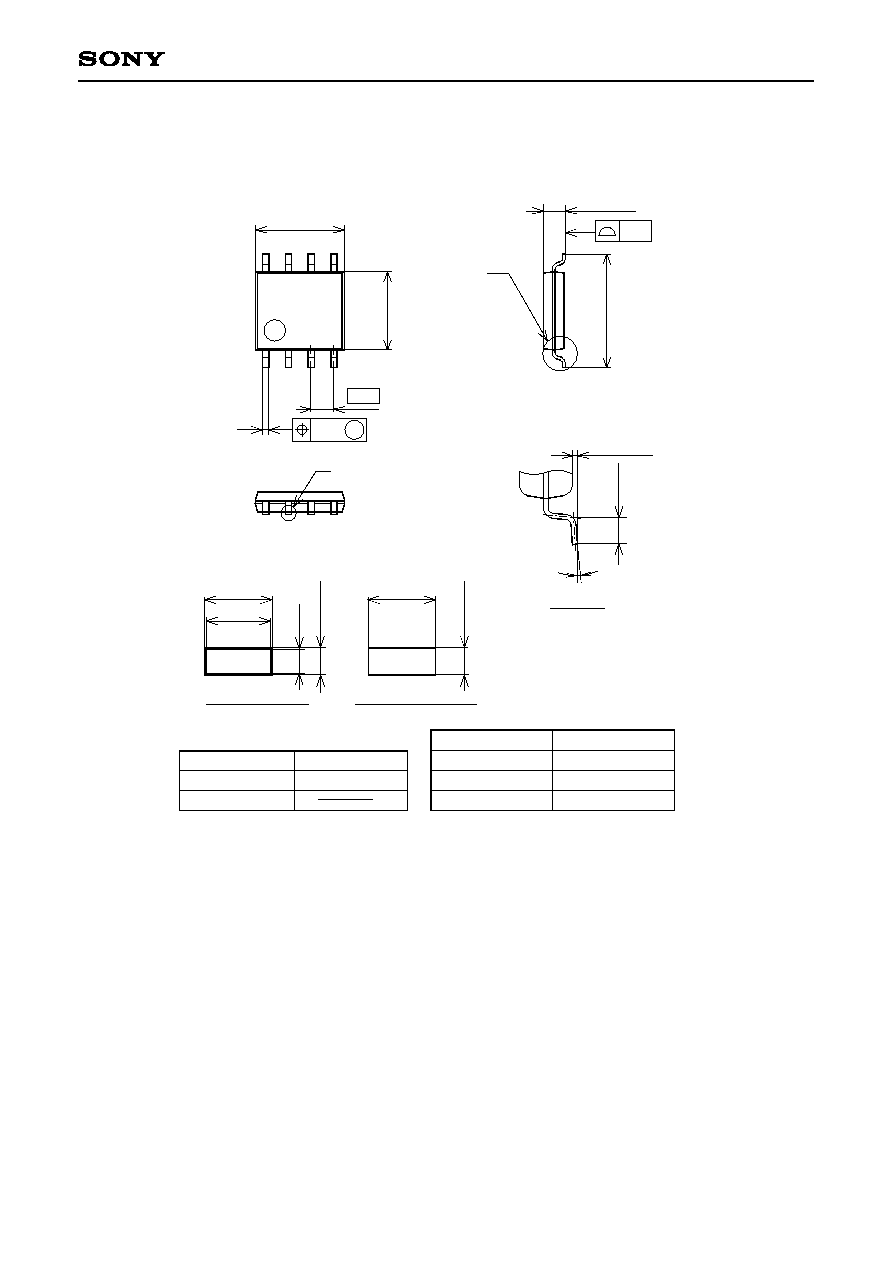
PACKAGE STRUCTURE
PACKAGE MATERIAL
LEAD TREATMENT
LEAD MATERIAL
PACKAGE MASS
EPOXY RESIN
SOLDER/PALLADIUM
42/COPPER ALLOY
0.1g
SOP-8P-L03
SOP008-P-0225
8PIN SOP (PLASTIC)
SONY CODE
EIAJ CODE
JEDEC CODE
0∞ to 10∞
0.1 ≠ 0.1
+ 0.15
0
.
5
±
0
.
2
DETAILA
8
5
1
4
4
.
4
≠
0
.
1
+
0
.
3
1.27
1.25 ≠ 0.15
+ 0.4
6
.
4
±
0
.
4
A
5.0 ≠ 0.1
+ 0.4
0.10
PLATING
M
0.24
b
B
(
0
.
1
5
)
0
.
1
5
≠
0
.
0
5
(0.4)
b = 0.4 ≠ 0.05
DETAIL B : SOLDER
0
.
1
5
≠
0
.
0
1
b = 0.4 ± 0.03
DETAIL B : PALLADIUM
+
0
.
0
3
+ 0.1
+
0
.
1
NOTE : PALLADIUM PLATING
This product uses S-PdPPF (Sony Spec.-Palladium Pre-Plated Lead Frame).
Package Outline
Unit: mm