 | –≠–Ľ–Ķ–ļ—ā—Ä–ĺ–Ĺ–Ĺ—č–Ļ –ļ–ĺ–ľ–Ņ–ĺ–Ĺ–Ķ–Ĺ—ā: CXA3299TN | –°–ļ–į—á–į—ā—Ć:  PDF PDF  ZIP ZIP |

--1--
E98Z30-TE
Sony reserves the right to change products and specifications without prior notice. This information does not convey any license by
any implication or otherwise under any patents or other right. Application circuits shown, if any, are typical examples illustrating the
operation of the devices. Sony cannot assume responsibility for any problems arising out of the use of these circuits.
Absolute Maximum Ratings (Ta=25 įC)
∑ Supply voltage
V
CC
6
V
∑ Operating temperature
Topr
≠20 to +70
įC
∑ Storage temperature
Tstg
≠55 to +150
įC
∑ Allowable power dissipation (on board)
P
D
1000
mW
Operating Conditions
Supply voltage
V
CC
3.2 to 5.5
V
Description
The CXA3299TN is a wideband Pre-amplifier for
VTR head.
Features
∑ Operate on single +3.3 V power supply
∑ Low power consumption
Read : 58 mW
∑ Ultra small package
∑ Wideband (≠3 dB) : 160 MHz (typ)
∑ Read amplifier emitter follower output featuring
380 times gain (typ).
∑ Low input capacitance : 3.0 pF
∑ Low input noise : 0.65 nV /
Hz
Structure
Bipolar silicon monolithic IC
Wideband Pre-amplifier
10 pin TSSOP (Plastic)
CXA3299TN
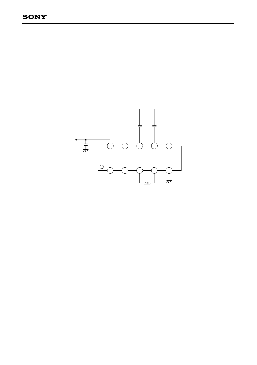
Block Diagram and Pin Configuration
NC
HX
HY
GND
NC
RDY
RDX
V
CC
NC
NC
AMP
1
2
3
4
5
10
9
8
7
6

--2--
CXA3299TN
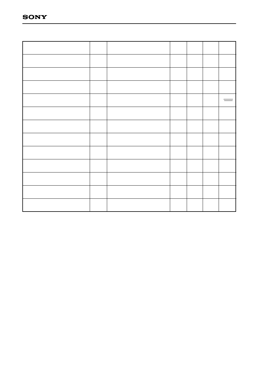
Pin Description
No.
Symbol
Equivalent circuit
Description
1
2
3
4
5
6
7
8
9
10
NC
H0X
H0Y
GND
NC
RDY
RDX
NC
V
CC
Head.
Read amplifier output.
4k
4k
V
CC
GND
100k
4
3
V
CC
GND
7
8
--3--
CXA3299TN
Electrical Characteristics
(Unless otherwise specified, V
CC
=3.3 V, Ta=25 įC)
Item
Current consumption for read
Read amplifier differential
voltage gain
Frequency band width
(≠3 dB)
Input referred noise voltage
Common mode rejection ratio
Supply voltage rejection ratio
Read data output offset voltage
for Read
Differential input capacitance
Differential input resistance
Output resistance
Read data output sink current
Read data output voltage
Symbol
I
CC
A
V
B
W
E
N
CMRR
PSRR
V
OFFR
C
IN
R
IN
R
RD
Isink
V
RD
Test condition
Input voltage :
1 mVp-p, 300 kHz
Frequency at which A
V
lower
by 3 dB
Head impedance : 0
Common input voltage :
100 mVp-p, 20 MHz
Ripple voltage :
100 mVp-p, 20 MHz
V
OFFR
=V
RDX
≠V
RDY
Min.
Typ.
Max.
Unit.
13.5
17.5
22.5
mA
300
380
460
V/V
100
160
MHz
0.65
0.8
nV
Hz
50
dB
50
dB
≠300
300
mV
3.0
4.5
pF
0.7
1.8
3.0
k
4
8
2.5
3.2
4.3
mA
V
CC
V
≠1.6
Guaranteed until Ta=70 įC

--4--
CXA3299TN
Test Circuit 1
◊
100
◊
1
b
a
1Ķ
1k
1Ķ
1k
AMP
V
AMP
V
LPF
V
V
b
a
a
b
a
b
a
b
c
b
a
d
0.1Ķ
1
2
3
4
5
c
b
a
d
A
0.1Ķ
0.1Ķ
A
to 50MHz
9
10
6
7
8
V
CC
3.3V
V
CC
3.3V
1Ķ
Test Circuit 2
◊
1
1Ķ
1k
1Ķ
1k
AMP
L
H
1ĶH
1
2
3
4
5
9
10
8
7
6
1Ķ
3.3V
Description of Functions
Pre-amplifier
This is a low noise amplifier for amplifying the signals from the heads with an emitter follower output.
The RDX and RDY are the outputs of the differential amplifier whose polarity between the RDX and X side of
the head input is same.
--5--
CXA3299TN
Application Circuit
1Ķ
1Ķ
L
H
1Ķ
9
10
6
7
8
1
2
3
4
5
3.3V
Application circuits shown are typical examples illustrating the operation of the devices. Sony cannot assume responsibility for
any problems arising out of the use of these circuits or for any infringement of third party patent and other right due to same.

--6--
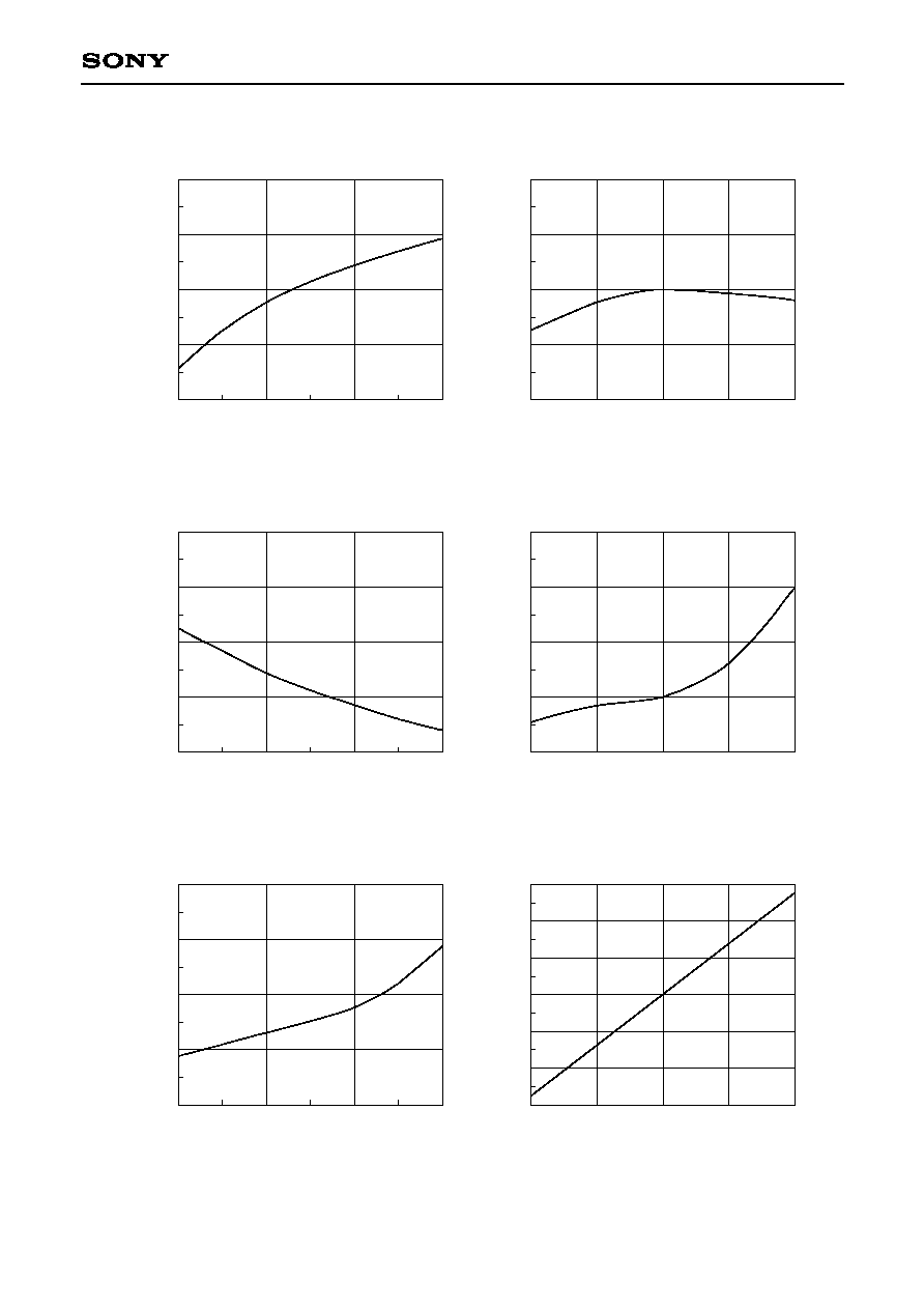
CXA3299TN
Normalized current consumption
vs. Supply voltage (Ta=25
į
C)
Supply voltage V
CC
[V]
I
CC
/I
CC
(V
CC
=3.3V)
Isink/Isink (V
CC
=3.3V)
A
v/A
v (V
CC
=3.3V)
1.10
1.08
1.06
1.04
1.02
1.00
0.98
0.96
3.0
4.0
5.0
6.0
Normalized current consumption
vs. Ambient temperature (V
CC
=3.3V)
Ambient temperature Ta [
į
C]
I
CC
/I
CC
(T
a=25
į
C)
1.10
1.05
1.00
0.95
0.90
≠25
0
25
50
75
Normalized read amplifier differential voltage gain
vs. Supply voltage (Ta=25
į
C)
Supply voltage V
CC
[V]
1.10
1.08
1.06
1.04
1.02
1.00
0.98
0.96
3.0
4.0
5.0
6.0
Normalized read amplifier differential voltage gain
vs. Ambient temperature (V
CC
=3.3V)
Ambient temperature Ta [
į
C]
A
v/A
v (T
a=25
į
C)
1.10
1.05
1.00
0.95
0.90
≠25
0
25
50
75
Normalized read data output sink current
vs. Supply voltage (Ta=25
į
C)
Supply voltage V
CC
[V]
1.10
1.08
1.06
1.04
1.02
1.00
0.98
3.0
4.0
5.0
6.0
Normalized read data output sink current
vs. Ambient temperature (V
CC
=3.3V)
Ambient temperature Ta [
į
C]
Isink/Isink (T
a=25
į
C)
1.04
1.02
1.00
0.98
0.96
≠25
0
25
50
75

--7--
CXA3299TN
Normalized frequency band width (≠3dB)
vs. Supply voltage (Ta=25
į
C)
Supply voltage V
CC
[V]
BW/BW (V
CC
=3.3V)
CMRR/CMRR (V
CC
=3.3V)
1.04
1.02
1.00
0.98
0.96
3.0
4.0
5.0
6.0
Normalized input referred noise voltage
vs. Supply voltage (Ta=25
į
C)
Supply voltage V
CC
[V]
En/En (V
CC
=3.3V)
1.04
1.02
1.00
0.98
0.96
3.0
4.0
5.0
6.0
Normalized frequency band width (≠3dB)
vs. Ambient temperature (V
CC
=3.3V)
Ambient temperature Ta [
į
C]
BW/BW (T
a=25
į
C)
1.10
1.05
1.00
0.95
0.90
≠25
0
25
50
75
Normalized common mode rejection ratio
vs. Supply voltage (Ta=25
į
C)
Supply voltage V
CC
[V]
1.06
1.04
1.02
1.00
0.98
0.96
0.94
3.0
4.0
5.0
6.0
Normalized common mode rejection ratio
vs. Ambient temperature (V
CC
=3.3V)
Ambient temperature Ta [
į
C]
CMRR/CMRR (T
a=25
į
C)
1.04
1.02
1.00
0.98
0.96
≠25
0
25
50
75
Normalized input referred noise voltage
vs. Ambient temperature (V
CC
=3.3V)
Ambient temperature Ta [
į
C]
En/En (T
a=25
į
C)
1.10
1.05
1.00
0.95
0.90
≠25
0
25
50
75
--8--
CXA3299TN
Normalized power supply rejection ratio
vs. Supply voltage (Ta=25
į
C)
Supply voltage V
CC
[V]
PSRR/PSRR (V
CC
=3.3V)
Rin/Rin (V
CC
=3.3V)
1.06
1.04
1.02
1.00
0.98
3.0
4.0
5.0
6.0
Normalized differential input capacitance
vs. Supply voltage (Ta=25
į
C)
Supply voltage V
CC
[V]
Cin/Cin (V
CC
=3.3V)
1.2
1.1
1.0
0.9
0.8
1.06
1.04
1.02
1.00
0.98
3.0
4.0
5.0
6.0
Normalized power supply rejection ratio
vs. Ambient temperature (V
CC
=3.3V)
Ambient temperature Ta [
į
C]
PSRR/PSRR (T
a=25
į
C)
1.02
1.01
1.00
0.99
0.98
≠25
0
25
50
75
Normalized differential input resistance
vs. Supply voltage (Ta=25
į
C)
Supply voltage V
CC
[V]
3.0
4.0
5.0
6.0
Normalized differential input resistance
vs. Ambient temperature (V
CC
=3.3V)
Ambient temperature Ta [
į
C]
Rin/Rin (T
a=25
į
C)
1.15
1.05
1.10
1.00
0.90
0.95
0.85
≠25
0
25
50
75
Normalized differential input capacitance
vs. Ambient temperature (V
CC
=3.3V)
Ambient temperature Ta [
į
C]
Cin/Cin (T
a=25
į
C)
1.15
1.10
1.05
1.00
0.95
≠25
0
25
50
75

--9--
CXA3299TN
Normalized output resistance
vs. Supply voltage (Ta=25
į
C)
Supply voltage V
CC
[V]
RRD/RRD (V
CC
=3.3V)
1.02
1.00
0.98
0.96
0.94
3.0
4.0
5.0
6.0
Normalized output resistance
vs. Ambient temperature (V
CC
=3.3V)
Ambient temperature Ta [
į
C]
RRD/RRD (T
a=25
į
C)
1.20
1.10
1.00
0.90
0.80
≠25
0
25
50
75

SONY CODE
EIAJ CODE
JEDEC CODE
PACKAGE MATERIAL
LEAD TREATMENT
LEAD MATERIAL
PACKAGE MASS
EPOXY RESIN
SOLDER PLATING
COPPER ALLOY
PACKAGE STRUCTURE
0.22 ≠ 0.07
0.5
5
1.2MAX
2.8 Ī 0.1
10
6
2.2 Ī
0.1
3.2 Ī
0.2
0.1 ≠ 0.05
+ 0.15
0.45 Ī
0.15
0į to 10į
1
A
(0.2)
0.22 ≠ 0.07
+ 0.08
(0.1)
0.12 ≠ 0.015
+ 0.025
DETAIL A
0.02g
TSSOP-10P-L01
10PIN TSSOP(PLASTIC)
0.1
0.1
M
NOTE: Dimension "
" does not include mold protrusion.
0.25
+ 0.08
Package Outline Unit : mm
CXA3299TN
--10--