 | –≠–ª–µ–∫—Ç—Ä–æ–Ω–Ω—ã–π –∫–æ–º–ø–æ–Ω–µ–Ω—Ç: CXB1577Q | –°–∫–∞—á–∞—Ç—å:  PDF PDF  ZIP ZIP |
≠ 1 ≠
CXB1577Q
E96Z24-PS
Post-Amplifier for Optical Fiber Communication Receiver
Description
The CXB1577Q achieves the 2R optical-fiber
communication receiver functions (Reshaping and
Regenerating) on a single chip. This IC is equipped
with the signal detection function, which is used to
enable TTL/ECL outputs. Also, the output disable
function performs the output shutdown. 3.3V/5.0V
can be used for the supply voltage.
Features
∑ Output disable function (TTL input)
∑ Signal detection function (TTL/ECL output)
∑ Supply voltage supports both 3.3V/5.0V
Applications
∑ SONET/SDH:
622.08Mbps
∑ Fibre Channel:
531.25Mbps
:
1.062Gbps
∑ Gigabit-Ethernet: 1.25Gbps
Absolute maximum Ratings
∑ Supply voltage
V
CC
≠ V
EE
≠0.3 to +7
V
∑ Storage temperature
Tstg
≠65 to +150
∞C
∑ Input voltage difference
V
D
≠ V
D
Vdif
0 to +2
V
∑ SW input voltage
Vi
V
EE
to V
CC
V
∑ ECL output current
I
O
Q/SD-ECL
≠30 to 0
mA
∑ TTL output current (High level)
I
OH
SD-TTL
≠20 to 0
mA
∑ TTL output current (Low level)
I
OL
SD-TTL
0 to 20
mA
Recommended Operating Conditions
∑ Supply voltage
V
CC
≠ V
EE
3.3 ± 0.2/5 ± 0.25
V
∑ Termination voltage (for data)
V
CC
≠ VT
D
1.8 to 2.2
V
∑ Termination voltage (for alarm 1,alarm 2)
VTA
V
EE
V
∑ Termination resistance (for data)
RT
D
46 to 56
∑ Termination resistance (for alarm 1)
RTA1
240 to 300
∑ Termination resistance (for alarm 2)
RTA2
460 to 560
∑ Operating temperature
Ta
≠40 to +85
∞C
Structure
Bipolar silicon monolithic IC
Sony reserves the right to change products and specifications without prior notice. This information does not convey any license by
any implication or otherwise under any patents or other right. Application circuits shown, if any, are typical examples illustrating the
operation of the devices. Sony cannot assume responsibility for any problems arising out of the use of these circuits.
40 pin QFP (Plastic)
--
--
≠ 2 ≠
CXB1577Q
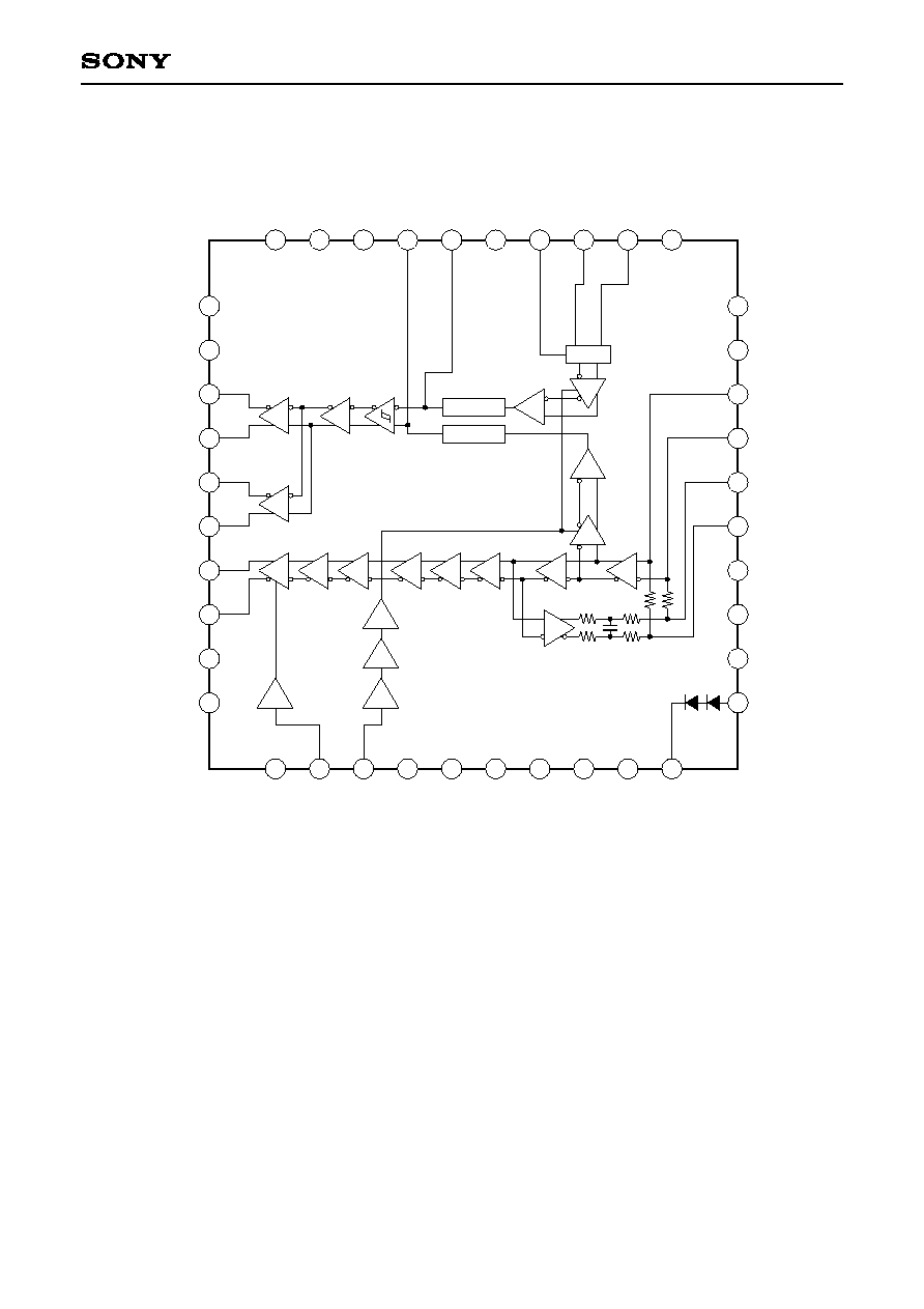
Block Diagram and Pin Configuration
V
E
E
4
2
3
4
5
6
7
8
9
10
11
12
13
14
15
16
17
18
19
20
21
22
23
24
25
26
27
28
29
30
40
39
38
37
36
35
34
31
32
33
1
N.C.
V
E
E
3
O
D
I
S
S
W
V
C
2
N
.
C
.
N
.
C
.
V
E
E
1
V
E
E
2
N
.
C
.
N
.
C
.
V
C
3
C
A
P
3
C
A
P
2
V
E
E
2
V
E
E
I
D
N
U
P
N
.
C
.
V
CC
3
QB
Q
VC1
SDB-ECL
SDB-TTL
SD-TTL
V
CC
4
TM
V
CC
1
N.C.
CAP1B
CAP1
D
V
CC
2
V
C
C
2
VC0
DB
V
EE
1
SD-ECL
peak hold
peak hold
V

≠ 3 ≠
CXB1577Q
Pin Description
Pin
No.
1
V
EE
3
≠3.3V
/ ≠5V
Negative power supply for ECL
output buffer.
Switches the identification
maximum voltage amplitude.
High voltage when open; the
identification maximum voltage
amplitude becomes 40mVp-p.
Low voltage when connected
to V
EE
; the amplitude becomes
20mVp-p.
2
ODIS
0V
(Open)
or
≠3.3V
/ ≠5V
3
SW
0V
(Open)
or
≠3.3V
/ ≠5V
Switches 3.3V/5V. Short this pin
to Vcc for 3.3V between Vcc and
V
EE
. Leave this pin open for 5V
between Vcc and V
EE
.
No connected.
Negative power supply for digital
block.
Negative power supply for analog
block.
Chip temperature monitor.
4
V
CC
2
0V
6
VC2
0V
/≠1.7V
(Open)
7
N.C.
8
9
10
5
V
EE
2
≠3.3V
/ ≠5V
V
EE
1
≠3.3V
/ ≠5V
11
TM
≠1.8V
/ ≠3.5V
Controls the output shutdown
function. High voltage when
open; the Q output is fixed to
Low. Low voltage when
connected to V
EE
; the D input
results in the Q output with ECL
level. TTL level is also available.
Symbol
Typical pin
voltage
DC
AC
Equivalent circuit
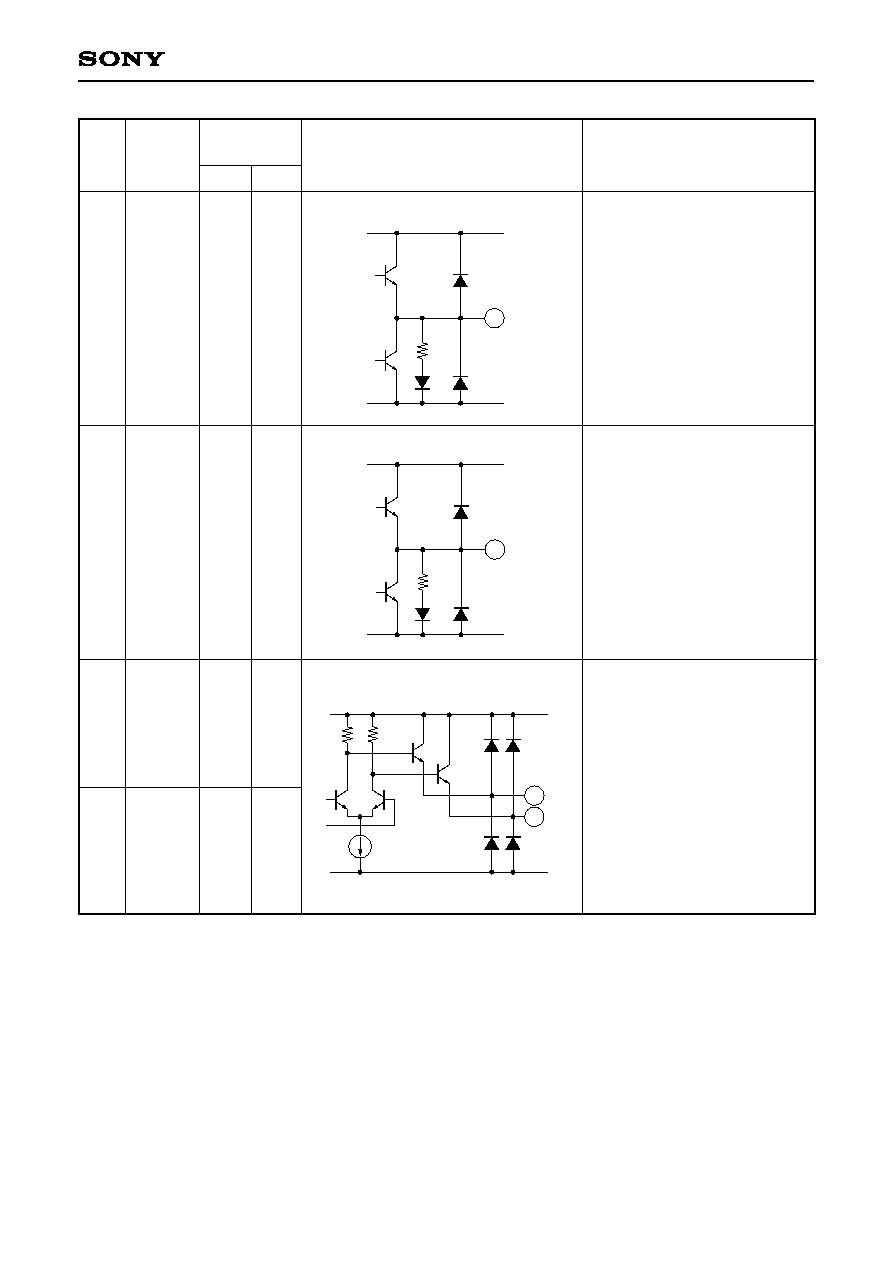
Description
V
CC
2
V
EE
2
40k
60k
3
2
V
CC
2
V
EE
2
V
REF
10k
10k
300
5
V
CC
2
V
EE
2
6k
2k
Positive power supply for digital block.
10
11
V
EE
1

≠ 4 ≠
CXB1577Q
12
13
14
15
16
17
18
19
20
21
22
23
24
25
V
CC
1
VC0
N.C.
CAP1B
CAP1
DB
D
V
EE
1
V
CC
2
N.C.
UP
DN
V
EE
I
V
EE
2
0V
≠0.9V
to
≠1.7V
≠0.9V
to
≠1.7V
Positive power supply for analog block.
No connected.
Switches 3.3V/5V. Short this pin
to Vcc for 3.3V between Vcc and
V
EE
. Leave this pin open for 5V
between Vcc and V
EE
.
Pins 15 and 16 connect a
capacitor which determines the
cut-off frequency for DC
feedback block.
Pins 17 and 18 are input pins
for limiting amplifier block. Input
the signal with AC coupled.
DC
AC
V
CC
3
V
EE
3
6k
2k
13
Negative power supply for analog
block.
Positive power supply for digital block.
No connected.
Connects a resistor for alarm
level setting.
Default voltage can be generated
without an external resistor by
shorting the V
EE
I pin to V
EE
.
Generates the default voltage
between UP and DOWN.
The voltage (8.0mV for input
conversion) can be generated
between UP and DOWN (Pins
22 and 23) as alarm setting level
by connecting this pin to V
EE
.
≠1.3V
≠1.3V
≠3.3V
/≠5V
0V
≠3.3V
/≠5V
≠3.3V
/≠5V
16
15
1k
18
17
1k
V
CC
1
V
EE
1
200
7.5k
100p
200
7.5k
Pin
No.
Symbol
Typical pin
voltage
Equivalent circuit
Description
23
24
V
CC
2
V
EE
2
100
22
986
100
140.9
140.9
V
CS
SW
SW
Negative power supply for digital
block.
0V
/≠1.7V
(Open)

≠ 5 ≠
CXB1577Q
32
DC
AC
26
CAP2
≠1.8V
Connects a peak hold circuit
capacitor for alarm block.
470pF should be connected
to Vcc each.
CAP2 pin connects a peak
hold capacitor for alarm
level setting block.
CAP3 pin connects a peak
hold capacitor for limiting
amplifier signal.
26
V
CC
2
V
EE
2
80
200
5µA
10p
27
CAP3
≠1.8V
28
29
30
31
VC3
V
EE
4
N.C.
V
CC
4
0V
/
≠1.7V
(Open)
≠3.3V
/≠5V
0V
Switches 3.3V/5V. Short this pin
to Vcc for 3.3V between Vcc and
V
EE
. Leave this pin open for 5V
between Vcc and V
EE
.
V
CC
2
V
EE
2
80
200
5µA
10p
27
V
CC
3
V
EE
3
6k
2k
28
VC1
0V
≠1.7V
(Open)
Switches 3.3V/5V. Short this pin
to Vcc for 3.3V between Vcc and
V
EE
. Leave this pin open for 5V
between Vcc and V
EE
.
V
CC
3
V
EE
3
6k
2k
32
Pin
No.
Symbol
Typical pin
voltage
Equivalent circuit
Description
Negative power supply for TTL
output buffer.
No connected.
Positive power supply for TTL
output buffer.
≠ 6 ≠
CXB1577Q
DC
AC
33
SD-TTL
V
EE
or
V
EE
+
3V
Alarm signal TTL level output.
V
CC
4
V
EE
4
33
40k
34
SDB-TTL
V
EE
or
V
EE
+
3V
35
36
SD-ECL
SDB-ECL
≠0.9V
or
≠1.7V
≠0.9V
or
≠1.7V
Alarm signal ECL level output.
Terminate this pin in 510
to V
EE
at V
EE
= 5V; in 270
to V
EE
at V
EE
= 3.3V.
V
CC
4
V
EE
4
40k
34
36
35
V
CC
3
V
EE
3
Pin
No.
Symbol
Typical pin
voltage
Equivalent circuit
Description
Alarm signal TTL level output.

≠ 7 ≠
CXB1577Q
DC
AC
37
Q
≠0.9V
or
≠1.7V
Data signal output. Terminates
this pin in 50
to VTT =
Vcc≠2V.
V
CC
3
V
EE
3
38
37
38
QB
≠0.9V
or
≠1.7V
39
40
V
CC
3
N.C.
0V
Pin
No.
Symbol
Typical pin
voltage
Equivalent circuit
Description
Positive power supply for ECL
output buffer.
No connected.
≠ 8 ≠
CXB1577Q
Supply current
Q/QB High output voltage
Q/QB Low output voltage
SD-ECL/SDB-ECL High output voltage
SD-ECL/SDB-ECL Low output voltage
SD-TTL/SDB-TTL High output voltage 1
SD-TTL/SDB-TTL High output voltage 2
SD-TTL/SDB-TTL Low output voltage
SW High input voltage
SW Low input voltage
SW High input current
SW Low input current
ODIS High input voltage
ODIS Low input voltage
ODIS High input current
ODIS Low input current
D/DB input resistance
Electrical Characteristics
DC Characteristics
Item
I
EE
VOH
VOL
VOH-E
VOL-E
VOH-T1
VOH-T2
VOL-T
VIHSW
VILSW
IIHSW
IILSW
VIHOD
VILOD
IIHOD
IILOD
Rin
50
to VTT
Ta = 0 to +85∞C
When Vcc ≠ V
EE
= 5.0V,
510
to V
EE
;
when Vcc ≠ V
EE
= 3.3V,
270
to V
EE
Ta = 0 to +85∞C
IOH = ≠0.4mA,
V
CC
≠ V
EE
= 3.3V,
Ta = 0 to +85∞C
IOH = ≠0.4mA,
V
CC
≠ V
EE
= 5V,
Ta = 0 to +85∞C
IOL = 2mA
Ta = 0 to +85∞C
at SW pin Open: High
at ODIS pin Open: High
≠74
≠1100
≠1860
≠1100
≠1890
V
EE
+ 2.2
V
EE
+ 2.4
V
CC
≠ 0.5
V
EE
≠100
V
EE
+ 2.0
V
EE
≠400
765
≠51
1020
≠34
≠860
≠1620
≠860
≠1650
V
EE
+ 0.5
V
CC
V
EE
+ 0.5
10
V
CC
+ 0.5
V
EE
+ 0.8
20
1275
mA
mV
V
µA
V
µA
Symbol
Min.
Typ.
Max.
Unit
Conditions
V
CC
= GND, V
EE
= ≠5V ± 5%, Ta = ≠40 to +85∞C, VC0 to VC3 = open,
or V
CC
= GND, V
EE
= ≠3.3V ± 5%, Ta = ≠40 to +85∞C, VC0 to VC3 = GND
≠ 9 ≠
CXB1577Q
AC Characteristics
1
VUP ≠ VDOWN = 100mV, Vin = 100mVp-p (single ended), SW pin: High, peak hold capacitance (CAP2,
CAP3 pins) of 470pF, connect V
EE
I to V
EE
.
2
VUP ≠ VDOWN = 100mV, Vin = 1Vp-p (single ended), SW pin: High, peak hold capacitance (CAP2, CAP3
pins) of 470pF, connect V
EE
I to V
EE
.
3
Vin = 50mVp-p (single ended), SW pin: Low, peak hold capacitance of 470pF, connect V
EE
I to V
EE
.
4
Vin = 1Vp-p (single ended), SW pin: Low, peak hold capacitance of 470pF, connect V
EE
I to V
EE
.
Maximum input voltage amplitude
Amplifier gain (excluding the output buffer)
Identification maximum voltage
amplitude of alarm level
SD/SDB hysteresis width
Alarm setting level for default
Q/QB rise time
Q/QB fall time
SD-TTL/SDB-TTL rise time
SD-TTL/SDB-TTL fall time
SD-ECL/SDB-ECL rise time
SD-ECL/SDB-ECL fall time
Propagation delay time
SD response assert time
SD response deassert time
SD response assert time for alarm
level default
SD response deassert time for alarm
level default
Item
Vmax
GL
VmaxA1
VmaxA2
P1
P2
Vdef
TrQ
TfQ
TrSDT
TfSDT
TrSDE
TfSDE
TPD
Tas
Tdas
Tasd
Tdasd
single-ended input
SW pad: Low,
single-ended input
SW pad: Open High,
single-ended input
SW pin: Low,
at default alarm level
SW pin: Open High,
at default alarm level
UP/DOWN pin: open,
V
EE
I = V
EE
,
Differential voltage input
20% to 80%
50
to VTT
V
EE
+ 0.8V to V
EE
+ 2.0V
C
L
= 10pF
20% to 80%
When Vcc ≠ V
EE
= 5.0V,
510
to V
EE
,
when Vcc ≠ V
EE
= 3.3V,
270
to V
EE
1
2
3
4
1600
52
20
40
3
3
7.0
0.4
0
2.3
0
2.3
6
6
8.4
230
230
7
7
9.7
350
350
10
10
1.6
1.6
1.9
100
100
100
100
mVp-p
dB
mVp-p
dB
mV
ps
ns
µs
Symbol
Min.
Typ.
Max.
Unit
Conditions
V
CC
= GND, V
EE
= ≠5V ± 5%, Ta = ≠40 to +85∞C, VC0 to VC3 = open,
or V
CC
= GND, V
EE
= ≠3.3V ± 5%, Ta = ≠40 to +85∞C, VC0 to VC3 = GND
≠ 10 ≠
CXB1577Q
DC Electrical Characteristics Measurement Circuit
2
3
4
5
6
7
8
9
10
11
12
13
14
15
16
17
18
19
20
21
22
23
24
25
26
27
28
29
30
40
39
38
37
36
35
34
31
32
33
1
N.C.
V
E
E
3
O
D
I
S
S
W
V
C
2
N
.
C
.
N
.
C
.
V
E
E
1
V
E
E
2
N
.
C
.
N
.
C
.
V
E
E
4
V
C
3
C
A
P
3
C
A
P
2
V
E
E
2
V
E
E
I
D
N
U
P
N
.
C
.
V
CC
3
QB
Q
VC1
SDB-ECL
SDB-TTL
SD-TTL
V
CC
4
TM
V
CC
1
N.C.
CAP1B
CAP1
D
V
CC
2
V
C
C
2
VC0
DB
V
EE
1
SD-ECL
peak hold
peak hold
V
C3
C3
C1
C1
C2
V
D
V
EE
≠5.0V/≠3.3V
V
SW
V
ODIS
510
51
51
270
510
270
VTT
≠2V
When V
EE
= ≠5.0V: VC0 to VC3 = open
When V
EE
= ≠3.3V: VC0 to VC3 = Vcc

≠ 11 ≠
CXB1577Q
AC Electrical Characteristics Measurement Circuit
0.047µF
2
3
4
5
6
7
8
9
10
11
12
13
14
15
16
17
18
19
20
21
22
23
24
25
26
27
28
29
30
40
39
38
37
36
35
34
31
32
33
1
N.C.
V
E
E
3
O
D
I
S
S
W
V
C
2
N
.
C
.
N
.
C
.
V
E
E
1
V
E
E
2
N
.
C
.
N
.
C
.
V
E
E
4
V
C
3
C
A
P
3
C
A
P
2
V
E
E
2
V
E
E
I
D
N
U
P
N
.
C
.
V
CC
3
QB
Q
VC1
SDB-ECL
SDB-TTL
SD-TTL
V
CC
4
TM
V
CC
1
N.C.
CAP1B
CAP1
D
V
CC
2
V
C
C
2
VC0
DB
V
EE
1
SD-ECL
peak hold
peak hold
V
470p
470p
0.047µF
1µF
V
CC
+2V
When V
EE
= ≠3.0V: VC0 to VC3 = open
When V
EE
= ≠1.3V: VC0 to VC3 = Vcc
Z0 = 50
V
EE
≠3V/ ≠1.3V
Oscilloscope
50
input
Z0 = 50
Z0 = 50
Z0 = 50
Oscilloscope
Hi-Z input
R
EX1
≠ 12 ≠
CXB1577Q
Application Circuit
R
EX1
2
3
4
5
6
7
8
9
10
11
12
13
14
15
16
17
18
19
20
21
22
23
24
25
26
27
28
29
30
40
39
38
37
36
35
34
31
32
33
1
N.C.
V
E
E
3
O
D
I
S
S
W
V
C
2
N
.
C
.
N
.
C
.
V
E
E
1
V
E
E
2
N
.
C
.
N
.
C
.
V
E
E
4
V
C
3
C
A
P
3
C
A
P
2
V
E
E
2
V
E
E
I
D
N
U
P
N
.
C
.
V
CC
3
QB
Q
VC1
SDB-ECL
SDB-TTL
SD-TTL
V
CC
4
TM
V
CC
1
N.C.
CAP1B
CAP1
D
V
CC
2
V
C
C
2
VC0
DB
V
EE
1
SD-ECL
peak hold
peak hold
V
470p
51
0.047µF
V
IN
When V
EE
= ≠3.3V: VC0 to VC3 = Vcc
When V
EE
= ≠5.0V: VC0 to VC3 = open
470p
VTT
51
Signal Generator
51
VTT
1µF
0.047µF
51
VTT
V
EE
TTL
Input
VTT
≠2.0V
51
51
ECL Output
ECL Output
TTL Output
V
EE
Application circuits shown are typical examples illustrating the operation of the devices. Sony cannot assume responsibility for
any problems arising out of the use of these circuits or for any infringement of third party patent and other right due to same.
≠ 13 ≠
CXB1577Q
R1
15
16
17
R1
R2
R2
To IC interior
C1
C1
D
C2
18
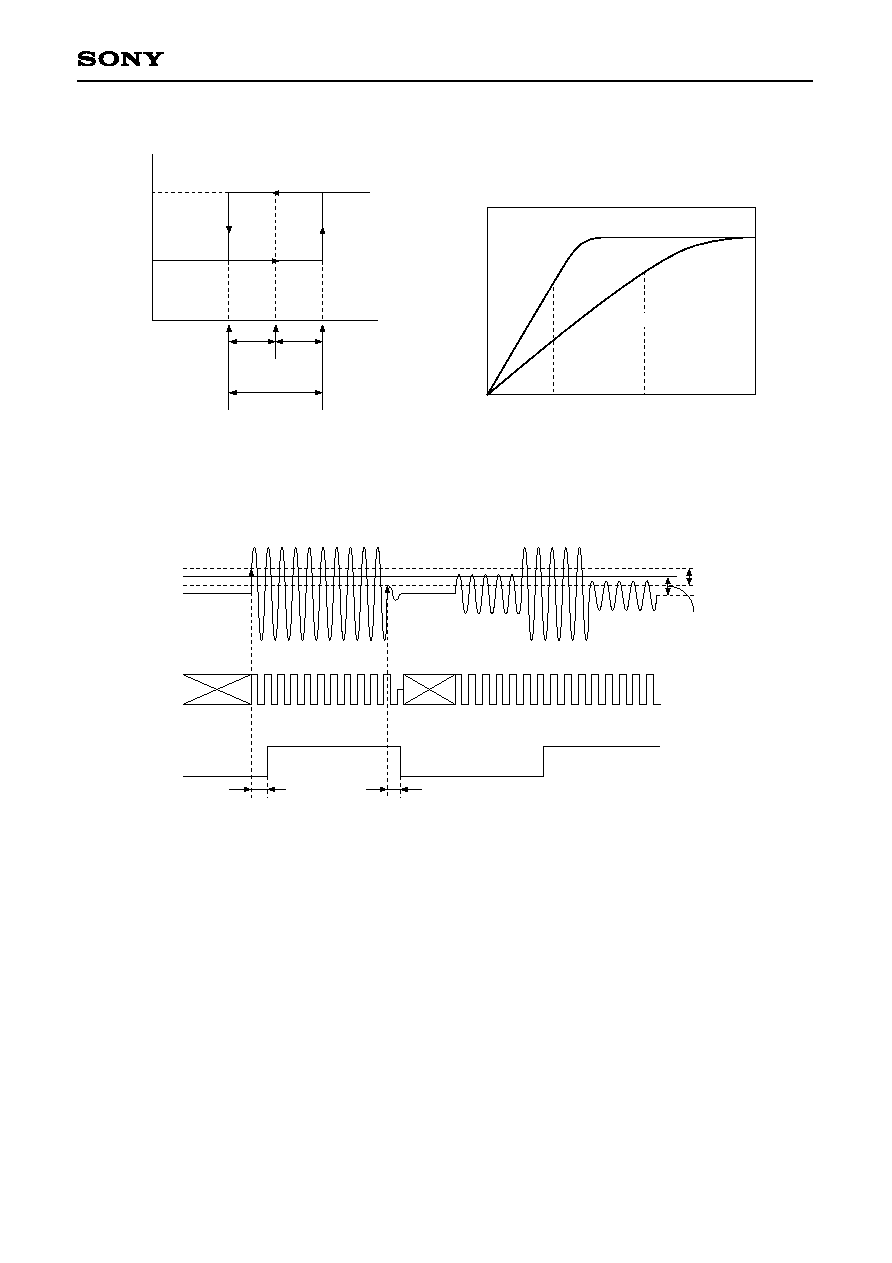
Fig. 1
Feedback frequency
response
f2
Amplifier frequency
response
f1
Frequency
G
a
i
n
Fig. 2
Notes on Operation
1. Limiting amplifier block
The limiting amplifier block is equipped with the auto-offset canceler circuit. When external capacitors C1 and
C2 are connected as shown in Fig. 1, the DC bias is set automatically in this block. External capacitor C1 and
IC internal resistor R1 determine the low input cut-off frequency f2 as shown in Fig. 2. Similarly, external
capacitor C2 and IC internal resistor R2 determine the high cut-off frequency f1 for DC bias feedback. Since
peaking characteristics may occur in the low frequency area of the amplifier gain characteristics depending on
the f1/f2 combination, set the C1 and C2 values so as to avoid the occurrence of peaking characteristics. The
target values of R1 and R2 and the typical values of C1 and C2 are as indicated below. When a single-ended
input is used, provide AC grounding by connecting Pin 17 to a capacitor which has the same capacitance as
capacitor C1.
R1 (internal): 1k
R2 (internal): 7.5k
f2: 3.4kHz
f1: 21Hz
C1 (external): 0.047µF
C2 (external): 1µF

≠ 14 ≠
CXB1577Q
2. Alarm block
In order to operate the alarm block, give the voltage difference between Pins 22 and 23 to set an alarm level
and connect the peak hold capacitor C3 shown in Fig. 3.
This IC has two setting methods of alarm level; one is to connect Pin 24 to V
EE
and leave Pins 22 and 23 open
to set an alarm level default value (8mV for input conversion). The other is to connect Pin 24 to V
EE
and set a
desired alarm level using the external resistors R
EX1
, R
EX2
and R
EX3
shown in Fig. 3. Connect R
EX1
between
Pins 22 and 23 or connect R
EX3
between Pin 23 and Vcc when less alarm level is desired to be set than its
default value; connect R
EX2
between Pin 22 and Vcc when more alarm level is desired to be set than its default
value. However, the Pin 22 voltage must be higher than that of Pin 23.
This IC also features two-level setting of identification maximum voltage amplitude. The amplitude is set to
40mVp-p when Pin 3 is left open (High level) and it is set to 20mVp-p when Pin 3 is Low level. Therefore, the
noise margin can be increased by setting Pin 3 to Low level when the small signal is input. The relation of input
voltage and peak hold output voltage is shown in Fig. 5.
In the relation between the alarm setting level and hysteresis width, the hysteresis width is designed to
maintain a constant gain (design target value: 6dB) as shown in Fig. 4.
This IC is designed to externally have the capacitor C3, and the C3 value should be set so as to obtain desired
assert time and deassert time settings for the alarm signal.
The electrical characteristics for the SD response assert and deassert times are guaranteed only when
the waveforms are input as shown in the timing chart of Fig. 6.
R
EX1
: 100
(when the alarm level is set to 4mV for input conversion.)
R
EX2
: 8k
(when the alarm level is set to 10mV for input conversion.)
R
EX3
: 4k
(when the alarm level is set to 4mV for input conversion.)
C3: 470pF
The table below shows the alarm logic.
The table below shows the output disable function logic.
V
CC
C3
V
CC
3
23
24
26
27
C3
Peak Hold
SD-TTL
SD-ECL
SDB-ECL
SDB-TTL
Peak Hold
V
10p
10p
V
CC
A
V
CC
A
From limiting amplifier
V
CC
R
EX3
R
EX1
R
EX2
V
CC
V
EE
22
23
24
Ra1
986
V
CC
A
IC interior
D
N
V
E
E
I
IC exterior
VCS
22
U
P
Ra2B
141
Ra2A
141
Ra1, Ra2A and Ra2B values are
typical values.
Optical signal input
state
Signal input
Signal interruption
Low level
High level
SD
High level
Low level
SD
Optical signal input
state
ODIS: Open High
ODIS: Low
Fixed High
Data
Q
Fixed Low
Data
Q
Fig. 3
≠ 15 ≠
CXB1577Q
Input electrical
signal amplitude
S
D
o
u
t
p
u
t
V
AS
V
DAS
3dB
3dB
Alarm setting
input level
Hysteresis
Large
Small
High
level
Low
level
V
DAS
Deassert level
V
AS
Assert level
Fig. 4
Input voltage [mVp-p]
P
e
a
k
h
o
l
d
o
u
t
p
u
t
v
o
l
t
a
g
e
SW
Low
0
20
40
SW
Open High
Fig. 5
Deassert time
Hysteresis width
Alarm setting level
Data input
(D)
Data output
(Q)
Assert time
Alarm output
(SD)
Fig. 6

≠ 16 ≠
CXB1577Q
1. Q/QB output waveform
Q
QB
Ch. 1 = 400mV/div OFFSET = ≠1330mV, Ch. 2 = 400mV/div OFFSET = ≠1330mV, Timebase = 500ps/div
V
CC
= GND
V
EE
= ≠3.3V
V
TT
= ≠2V
Ta = 27∞C
D = 622Mbps
Vin = 10mVp-p
Single input
pattern: PRBS2
23
-1
Q/QB = 50
to V
TT
Q
QB
Ch. 1 = 400mV/div OFFSET = ≠1330mV, Ch. 2 = 400mV/div OFFSET = ≠1330mV, Timebase = 200ps/div
V
CC
= GND
V
EE
= ≠3.3V
V
TT
= ≠2V
Ta = 27∞C
D = 1.25Gbps
Vin = 5mVp-p
Single input
pattern: PRBS2
23
-1
Q/QB = 50
to V
TT
Q
QB
Ch. 1 = 400mV/div OFFSET = ≠1330mV, Ch. 2 = 400mV/div OFFSET = ≠1330mV, Timebase = 500ps/div
V
CC
= GND
V
EE
= ≠3.3V
V
TT
= ≠2V
Ta = 27∞C
D = 622Mbps
Vin = 5mVp-p
Single input
pattern: PRBS2
23
-1
Q/QB = 50
to V
TT
Fig. 7
Fig. 8
Fig. 9
Example of Representative Characteristics

≠ 17 ≠
CXB1577Q
2. Bit error rate
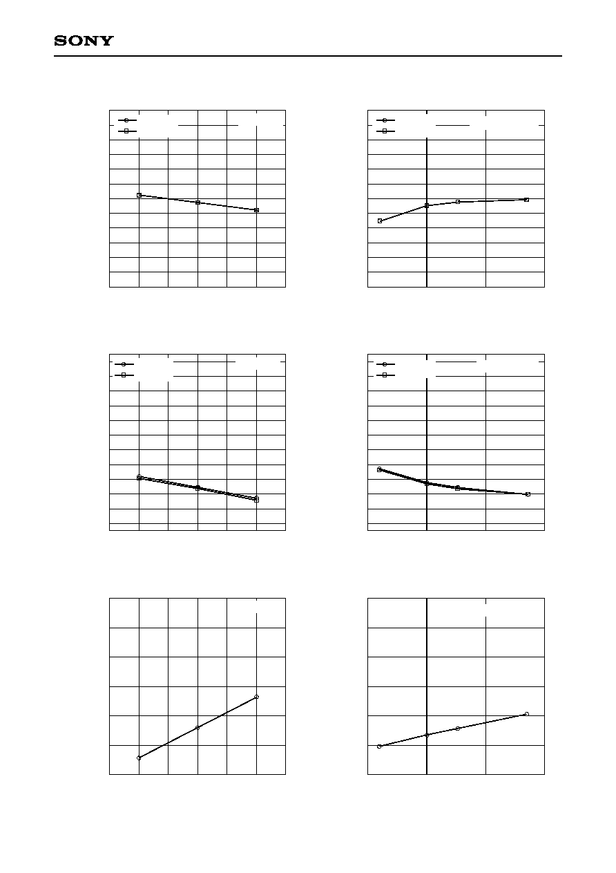
3. Alarm level
622Mbps
1.0Gbps
1.25Gbps
Bit error rate vs. Data input level
Data input level [mVp-p]
1.5
2
2.5
3
3.5
4
4.5
10
≠10
10
≠9
10
≠8
10
≠7
10
≠6
10
≠5
10
≠4
10
≠3
V
CC
= GND
V
EE
= ≠3.3V
V
TT
= ≠2V
Ta = 27∞C
Single input
pattern: PRBS2
23
-1
Q/QB = 50
to V
TT
B
i
t
e
r
r
o
r
r
a
t
e
Alarm level temperature
Ta [∞C]
≠40
2.0
20
80
A
l
a
r
m
l
e
v
e
l
[
m
V
]
2.5
3.0
3.5
4.0
4.5
5.0
6.0
SW = H
SW = L
fin = 100Mbps
V
CC
≠ V
EE
= 3.3V
Up-Down = 200
(R
EX1
)
≠20
40
0
60
5.5
Alarm level vs. R
EX1
UP-DOWN (REX1) [
]
10
2
2
10
3
10
4
A
l
a
r
m
l
e
v
e
l
[
m
V
]
3
4
5
6
7
8
9
SW = H
SW = L
fin = 100Mbps
V
CC
≠ V
EE
= 3.3V
Ta = 27∞C
Differential input
Q
QB
Ch. 1 = 400mV/div OFFSET = ≠1330mV, Ch. 2 = 400mV/div OFFSET = ≠1330mV, Timebase = 200ps/div
V
CC
= GND
V
EE
= ≠3.3V
V
TT
= ≠2V
Ta = 27∞C
D = 1.25Gbps
Vin = 10mVp-p
Single input
pattern: PRBS2
23
-1
Q/QB = 50
to V
TT
Fig. 10
Fig. 11
Fig. 12
Fig. 13

≠ 18 ≠
CXB1577Q
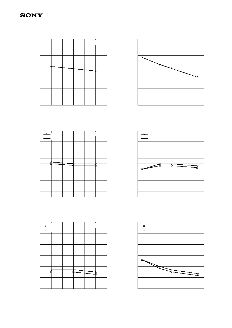
Alarm level supply voltage
V
CC
≠ V
EE
[V]
3.0
2.0
Fig. 14
3.3
3.6
A
l
a
r
m
l
e
v
e
l
[
m
V
]
2.5
3.0
3.5
4.0
4.5
5.0
6.0
SW = H
SW = L
fin = 100Mbps
Ta = 27∞C
Up-Down = 200
(REX1)
3.1
3.4
3.2
3.5
5.5
Alarm level temperature
Ta [∞C]
≠40
11.0
20
80
A
l
a
r
m
l
e
v
e
l
[
m
V
]
11.5
12.0
12.5
13.0
13.5
14.0
15.0
SW = H
SW = L
fin = 100Mbps
V
CC
≠ V
EE
= 3.3V
V
CC
-UP = 5k
(R
EX2
)
≠20
40
0
60
14.5
Alarm level supply voltage
V
CC
≠ V
EE
[V]
3.0
11.0
3.3
3.6
A
l
a
r
m
l
e
v
e
l
[
m
V
]
11.5
12.0
12.5
12.0
13.5
14.0
15.0
SW = H
SW = L
fin = 100Mbps
Ta = 27∞C
V
CC
-UP = 5k
(R
EX2
)
3.1
3.4
3.2
3.5
14.5
Alarm level vs. R
EX2
V
CC
-UP (R
EX2
) [
]
10
3
8
10
4
10
5
A
l
a
r
m
l
e
v
e
l
[
m
V
]
10
11
12
13
14
15
16
SW = H
SW = L
fin = 100Mbps
V
CC
≠ V
EE
= 3.3V
Ta = 27∞C
Differential input
9
Alarm level temperature
Ta [∞C]
≠40
2.5
20
80
A
l
a
r
m
l
e
v
e
l
[
m
V
]
3.0
3.5
4.0
4.5
5.0
6.0
SW = H
SW = L
fin = 100Mbps
V
CC
≠ V
EE
= 3.3V
V
CC
-Down = 3k
(R
EX3
)
≠20
40
0
60
5.5
Alarm level vs. R
EX3
V
CC
-DOWN (R
EX3
) [
]
10
3
3
10
4
10
5
A
l
a
r
m
l
e
v
e
l
[
m
V
]
4
5
6
7
8
9
SW = H
SW = L
fin = 100Mbps
V
CC
≠ V
EE
= 3.3V
Ta = 27∞C
Differential input
Fig. 15
Fig. 16
Fig. 17
Fig. 18
Fig. 19

≠ 19 ≠
CXB1577Q
Alarm level supply voltage
V
CC
≠ V
EE
[V]
3.0
2.0
3.3
3.6
A
l
a
r
m
l
e
v
e
l
[
m
V
]
2.5
3.0
3.5
4.0
4.5
5.0
6.0
SW = H
SW = L
fin = 100Mbps
Ta = 27∞C
V
CC
-Down = 3k
(R
EX3
)
3.1
3.4
3.2
3.5
5.5
Hyteresis width supply voltage
V
CC
≠ V
EE
[V]
3.0
0.0
3.3
3.6
H
Y
S
[
d
B
]
1.0
2.0
3.0
4.0
5.0
6.0
8.0
SW = H
SW = L
fin = 100Mbps
Ta = 27∞C
Up, Down = Open
V
EE
I = V
EE
3.1
3.4
3.2
3.5
7.0
Hysteresis width vs. Alarm level
Alarm level [mV]
2.0
0.0
8.0
14.0
H
Y
S
[
d
B
]
1.0
2.0
3.0
4.0
5.0
6.0
8.0
SW = H
SW = L
fin = 100Mbps
V
CC
≠ V
EE
= 3.3V
Ta = 27∞C
4.0
10.0
6.0
12.0
7.0
Hysteresis width temperature
Ta [∞C]
≠40
0.0
20
80
H
Y
S
[
d
B
]
2.0
3.0
4.0
5.0
6.0
8.0
SW = H
SW = L
fin = 100Mbps
V
CC
≠ V
EE
= 3.3V
Up, Down = Open
V
EE
I = V
EE
≠20
40
0
60
7.0
1.0
Alarm level vs. Data rate
fin [Mbps]
200
2
800
1400
A
l
a
r
m
l
e
v
e
l
[
m
V
]
6
8
10
12
14
16
SW = H
SW = L
V
CC
≠ V
EE
= 3.3V
Ta = 27∞C
Up, Down = Open
V
EE
I = V
EE
400
1000
600
1200
4
0
Hysteresis width vs. Data rate
fin [Mbps]
200
0
800
1400
H
Y
S
[
d
B
]
4
6
8
10
12
SW = H
SW = L
V
CC
≠ V
EE
= 3.3V
Ta = 27∞C
Up, Down = Open
V
EE
I = V
EE
400
1000
600
1200
2
0
Fig. 20
Fig. 21
Fig. 22
Fig. 23
Fig. 24
Fig. 25
≠ 20 ≠
CXB1577Q
SD-ECL "H" level supply voltage
V
CC
≠ V
EE
[V]
3.0
≠1100
3.3
3.6
"
H
"
l
e
v
e
l
[
m
V
]
≠1060
≠1020
≠980
≠940
≠900
≠860
SD-ECL
SDB-ECL
Ta = 27∞C
3.1
3.4
3.2
3.5
SD-ECL "L" level temperature
Ta [∞C]
≠50
100
SD-ECL
SDB-ECL
V
CC
≠ V
EE
= 3.3V
50
0
≠1880
"
L
"
l
e
v
e
l
[
m
V
]
≠1840
≠1800
≠1760
≠1720
≠1680
SD-ECL "L" level supply voltage
V
CC
≠ V
EE
[V]
3.0
≠1880
3.3
3.6
"
L
"
l
e
v
e
l
[
m
V
]
≠1840
≠1800
≠1760
≠1720
≠1680
SD-ECL
SDB-ECL
Ta = 27∞C
3.1
3.4
3.2
3.5
SD-ECL "H" level temperature
Ta [∞C]
≠50
100
SD-ECL
SDB-ECL
V
CC
≠ V
EE
= 3.3V
50
0
≠1100
"
H
"
l
e
v
e
l
[
m
V
]
≠1060
≠1020
≠980
≠940
≠900
≠860
SD-TTL "H" level supply voltage
V
CC
≠ V
EE
[V]
3.0
2.2
3.3
3.6
"
H
"
l
e
v
e
l
[
V
]
2.4
2.6
2.8
3.0
3.4
Ta = 27∞C
3.1
3.4
3.2
3.5
3.2
SD-TTL "H" level temperature
Ta [∞C]
≠50
100
V
CC
≠ V
EE
= 3.3V
50
0
2.2
"
H
"
l
e
v
e
l
[
V
]
2.4
2.6
2.8
3.0
3.4
3.2
4. DC voltage
Fig. 26
Fig. 27
Fig. 28
Fig. 29
Fig. 30
Fig. 31
≠ 21 ≠
CXB1577Q
SD-TTL "L" level temperature
Ta [∞C]
≠50
100
V
CC
≠ V
EE
= 3.3V
50
0
200
"
L
"
l
e
v
e
l
[
m
V
]
250
300
350
400
SD-TTL "L" level supply voltage
V
CC
≠ V
EE
[V]
3.0
200
3.3
3.6
"
L
"
l
e
v
e
l
[
m
V
]
250
300
350
400
Ta = 27∞C
3.1
3.4
3.2
3.5
Q "H" level supply voltage
V
CC
≠ V
EE
[V]
3.0
≠1100
3.3
3.6
"
H
"
l
e
v
e
l
[
m
V
]
≠1060
≠1020
≠980
≠940
≠900
≠860
Q-H
QB-H
Ta = 27∞C
3.1
3.4
3.2
3.5
Q "H" level temperature
Ta [∞C]
≠50
100
Q-H
QB-H
V
CC
≠ V
EE
= 3.3V
50
0
≠1100
"
H
"
l
e
v
e
l
[
m
V
]
≠1060
≠1020
≠980
≠940
≠900
≠860
Q "L" level supply voltage
V
CC
≠ V
EE
[V]
3.0
≠1860
3.3
3.6
"
L
"
l
e
v
e
l
[
m
V
]
≠1820
≠1780
≠1740
≠1700
≠1660
Q-L
QB-L
Ta = 27∞C
3.1
3.4
3.2
3.5
≠1620
Q "L" level temperature
Ta [∞C]
≠50
100
Q-L
QB-L
V
CC
≠ V
EE
= 3.3V
50
0
"
L
"
l
e
v
e
l
[
m
V
]
≠1860
≠1820
≠1780
≠1740
≠1700
≠1660
≠1620
Fig. 32
Fig. 33
Fig. 34
Fig. 35
Fig. 36
Fig. 37
≠ 22 ≠
CXB1577Q
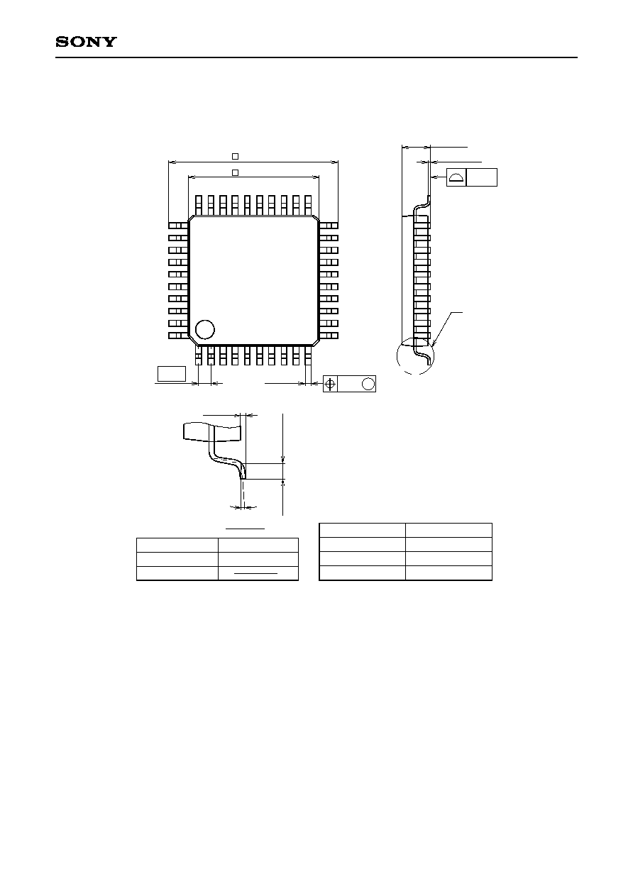
SONY CODE
EIAJ CODE
JEDEC CODE
PACKAGE MATERIAL
LEAD TREATMENT
LEAD MATERIAL
PACKAGE MASS
EPOXY RESIN
SOLDER / PALLADIUM
42/COPPER ALLOY
PACKAGE STRUCTURE
PLATING
0.2g
QFP-40P-L01
QFP040-P-0707
40PIN QFP (PLASTIC)
9.0 ± 0.4
+ 0.4
0.3 ≠ 0.1
1
10
11
20
21
30
31
40
1.5 ≠ 0.15
+ 0.35
0.127 ≠ 0.05
+ 0.1
(
8
.
0
)
A
A
DETAIL
0.1 ≠ 0.1
+ 0.15
+ 0.15
7.0 ≠ 0.1
0
.
5
±
0
.
2
0.1
M
± 0.12
0.65
NOTE : PALLADIUM PLATING
This product uses S-PdPPF (Sony Spec.-Palladium Pre-Plated Lead Frame).
Package Outline
Unit: mm