≠ 1 ≠
E00924A1Y-PS
Sony reserves the right to change products and specifications without prior notice. This information does not convey any license by
any implication or otherwise under any patents or other right. Application circuits shown, if any, are typical examples illustrating the
operation of the devices. Sony cannot assume responsibility for any problems arising out of the use of these circuits.
CXG1109EN
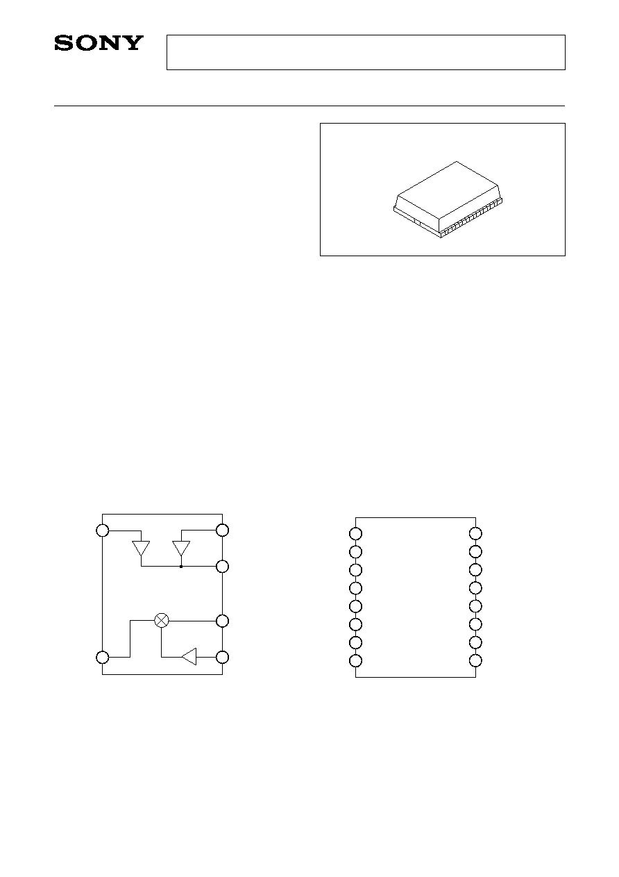
16 pin VSON (Plastic)
IF
OUT
LNA RF
IN
1
LO IN
LNA RF
IN
2
LNA RF
OUT
MIX RF
IN
1
3
6
8
9
16
IF
OUT
/V
DD
3 (MIX)
LNA RF
IN
1
CAP
GND
CTL
GND
GND
V
DD
2 (LO AMP)
LO IN
LNA RF
IN
2
CAP
GND
LNA RF
OUT
/V
DD
1 (LNA)
OPT
MIX RF
IN
GND
1
2
3
4
5
6
7
8
9
10
11
12
13
14
15
16
Receive Dual Low Noise Amplifier/Mixer
Description
The CXG1109EN is a receive dual low noise amplifier/
mixer MMIC. This IC is designed using the Sony's
GaAs J-FET process.
Features
∑ High conversion gain: Gp = 16.5 to 17dB (LNA Typ.)
Gc = 9.5 to 10dB (MIX Typ.)
∑ Low noise figure:
NF = 1.5dB (LNA Typ.)
NF = 4 to 5dB (MIX Typ.)
∑ Single 3V power supply operation
∑ Low LO input power operation P
LO
= ≠12.5dBm
∑ Single CTL pin achieved by the built-in inverter
circuit
∑ 16-pin VSON package
Applications
800MHz Japan digital cellular telephones (PDC)
Structure
GaAs J-FET MMIC
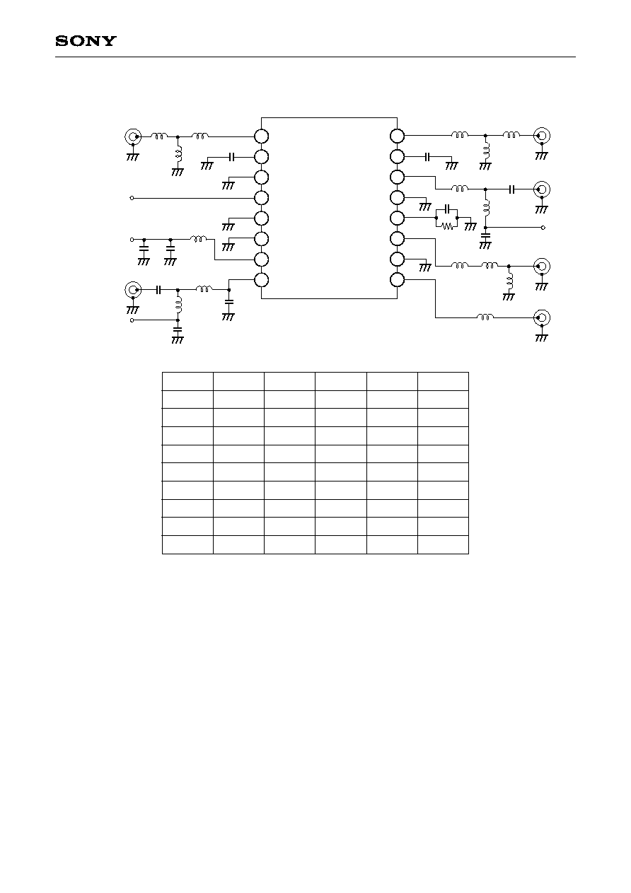
Block Diagram
Absolute Maximum Ratings (Ta = 25∞C)
∑ Supply voltage
V
DD
4.5
V
∑ Input power
P
IN
+13
dBm
∑ Current consumption
I
DD
15
mA
∑ Operating temperature Topr
≠35 to +85
∞C
∑ Storage temperature
Tstg
≠65 to +150
∞C
Recommended Operating Voltages
∑ Supply voltage
V
DD
2.7 to 3.3
V
∑ Control voltage
V
CTL
(H) 2.4 to 3.3
V
V
CTL
(L)
0 to 0.3
V
Pin Configuration
GaAs MMICs are ESD sensitive devices. Special handling precautions are required.

≠ 2 ≠
CXG1109EN
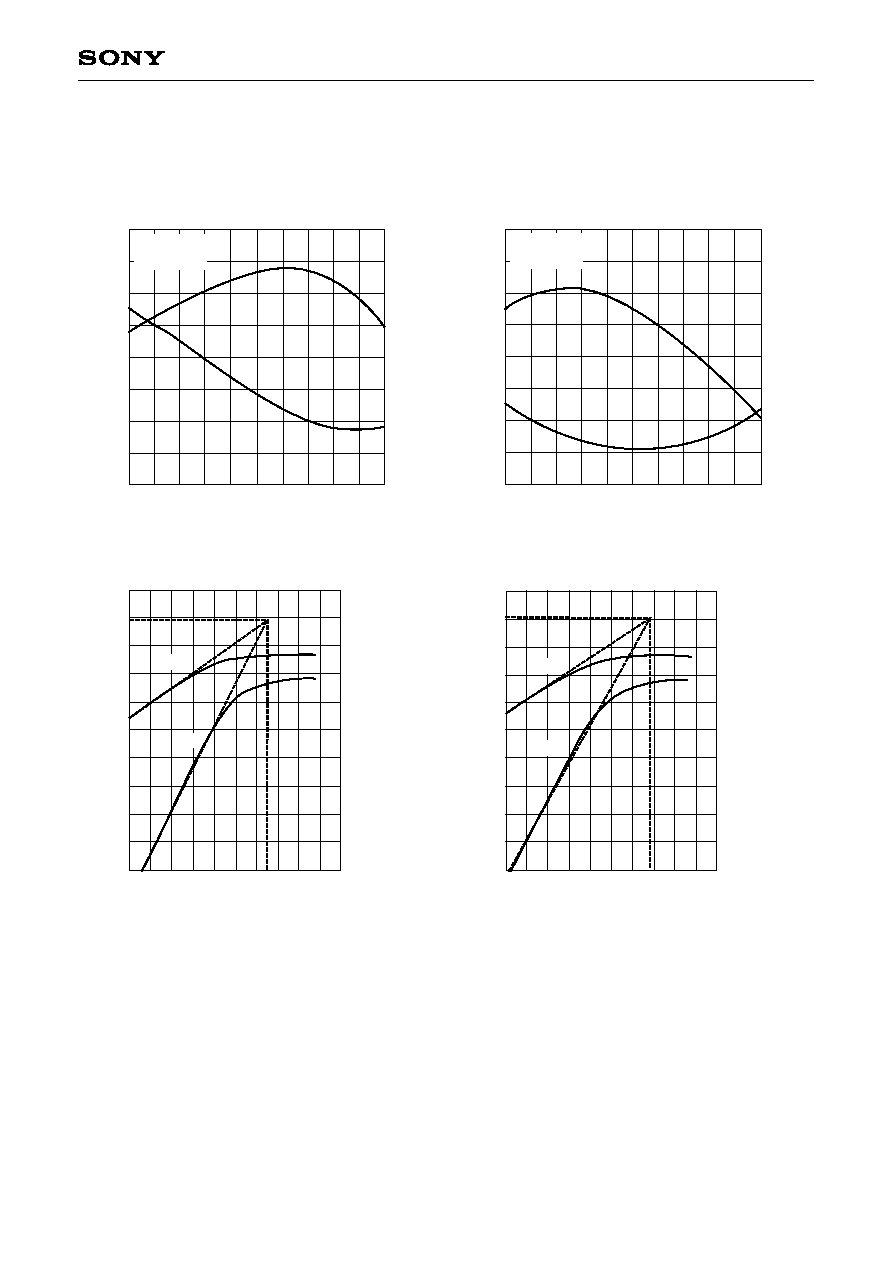
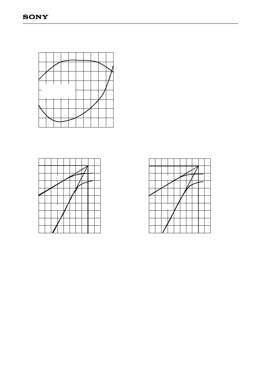
Electrical Characteristics
Conditions: V
DD
= 3.0V, V
CTL
(H) = 3.0V, V
CTL
(L) = 0V, f
RF
1 = 885MHz, f
RF
2 = 810MHz, f
LO
= f
RF
≠ 130MHz,
P
LO
= ≠12.5dBm, Ta = 25∞C, unless otherwise specified
Low Noise Amplifier Block
Mixer Block
The values shown above are the specified values on the Sony's recommended evaluation board.
1
Conversion from the IM3 suppression ratio for two-wave input: PRF = ≠30dBm (low noise amplifier block)/
≠22.5dBm (mixer block) at fRFoffset = 100kHz.
Current
consumption
Control current
Power gain
Noise figure
Input IP3
Isolation
Item
I
DD
I
CTL
Gp
NF
IIP3
I
SO
Symbol
--
--
RF
IN
1
RF
OUT
RF
IN
2
RF
OUT
RF
IN
1
RF
OUT
RF
IN
2
RF
OUT
RF
IN
1
RF
OUT
RF
IN
2
RF
OUT
RF
OUT
RF
IN
1
RF
OUT
RF
IN
2
Path
--
--
--
--
f
RF
1
f
RF
2
f
RF
1
f
RF
2
f
RF
1
f
RF
2
f
RF
1
f
RF
2
RF frequency
H
L
H
L
H
L
H
L
H
L
H
L
H
L
V
CTL
--
--
--
≠1
15
--
--
15
--
--
≠11
≠12.5
17
18
Min.
1.9
1.9
55
0
16.5
≠20
≠26
17
1.5
1.5
≠7.5
≠9
22
23
Typ.
2.5
2.5
80
--
19
≠15
≠21
19
2
2
--
--
--
--
Max.
mA
µA
dB
dB
dBm
dB
Unit
When no
signal
When a
small signal
1
When a
small signal
Measurement
condition
Item
Symbol
RF frequency
Min.
Typ.
Max.
Unit
Measurement condition
Current consumption
Power gain
Noise figure
Input IP3
LO to RF leak level
I
DD
G
C
NF
IIP3
Plk
--
f
RF
1
f
RF
2
f
RF
1
f
RF
2
f
RF
1
f
RF
2
f
RF
1
f
RF
2
--
9
8.5
--
--
≠1
≠1.5
--
--
4.5
10
9.5
5
4
1.5
1.5
≠22
≠24
6.2
11.5
11
6.5
5.5
--
--
≠17
≠19
mA
dB
dB
dBm
dBm
When no signal
When a small signal
1
f
LO
= 755MHz
f
LO
= 680MHz