 | –≠–Ľ–Ķ–ļ—ā—Ä–ĺ–Ĺ–Ĺ—č–Ļ –ļ–ĺ–ľ–Ņ–ĺ–Ĺ–Ķ–Ĺ—ā: BYW29 | –°–ļ–į—á–į—ā—Ć:  PDF PDF  ZIP ZIP |

1/7
BYW29/F/FP/G-200
ģ
May 2002 - Ed: 4B
HIGH EFFICIENCY FAST RECOVERY DIODES
I
F(AV)
8 A
V
RRM
200 V
trr (max)
25 ns
V
F
(max)
0.85 V
MAIN PRODUCT CHARACTERISTICS
s
Very Low Forward Losses
s
Negligible switching losses
s
High surge current capability
s
Insulated
packages
(ISOWATT220AC,
TO-220FPAC):
Insulation voltage: 2000 VDC
Typical insulation capacitance = 12 pF
FEATURES AND BENEFITS
Single rectifier suited for Switch Mode Power
Supply and high frequency DC to DC converters.
Packaged
in
TO-220AC,
ISOWATT220AC,
TO-220FPAC and D
2
PAK, this device is intended
for use in high frequency inverters, free wheeling
and polarity protection applications.
DESCRIPTION
NC
A
K
Symbol
Parameter
Value
Unit
V
RRM
Repetitive peak reverse voltage
200
V
I
F(RMS)
RMS forward current
16
A
I
F(AV)
Average forward current
= 0.5
D
2
PAK /
TO-220AC
Tc =120įC
8
A
ISOWATT220AC
TO-220FPAC
Tc = 100įC
I
FSM
Surge non repetitive forward current
(All pins connected)
tp=10ms
sinusoidal
80
A
Tstg
Storage and junction temperature range
- 65 to + 150
įC
Tj
Maximum operating junction temperature
+ 150
ABSOLUTE MAXIMUM RATINGS
D
2
PAK
BYW29G-200
TO-220AC
BYW29-200
TO-220FPAC
BYW29FP-200
ISOWATT220AC
BYW29F-200
A
K
K
A
K
A
K
A

BYW29/F/FP/G-200
2/7
Symbol
Parameter
Value
Unit
Rth (j-c)
Junction to case thermal resistance
TO-220AC
D2PAK
2.8
į
C/W
ISOWATT220AC
5
TO-220FPAC
5.5
THERMAL RESISTANCE
Symbol
Parameter
Test Conditions
Min.
Typ.
Max.
Unit
I
R
*
Reverse leakage current
V
R
= V
RRM
T
j
= 25įC
10
Ķ
A
T
j
= 100
į
C
0.6
mA
V
F **
Forward voltage drop
I
F
= 5 A
T
j
= 125
į
C
0.85
V
I
F
= 10 A
T
j
= 125
į
C
1.05
I
F
= 10 A
T
j
= 25
į
C
1.15
Pulse test :
* tp = 5 ms, duty cycle < 2 %
** tp = 380
Ķ
s, duty cycle < 2 %
To evaluate the conduction losses use the following equation :
P = 0.65 x I
F(AV)
+ 0.040 I
F
2
(RMS)
STATIC ELECTRICAL CHARACTERISTICS
Symbol
Parameter
Test Conditions
Min.
Typ.
Max.
Unit
t
rr
Reverse recovery
time
T
j
= 25įC
I
F
= 0.5A
Irr = 0.25 A
I
R
= 1A
25
ns
T
j
= 25
į
C
I
F
= 1A
dI
F
/dt = -50A/
Ķ
s
V
R
=
30V
35
t
fr
Forward recovery
time
T
j
= 25
į
C
I
F
= 1A
dI
F
/dt = 100A/
Ķ
s
V
FR
= 1.1 x V
F
max
15
ns
V
FP
Peak forward
voltage
T
j
= 25
į
C
I
F
= 1A
dI
F
/dt = 100A/
Ķ
s
2
V
RECOVERY CHARACTERISTICS
BYW29/F/FP/G-200
3/7
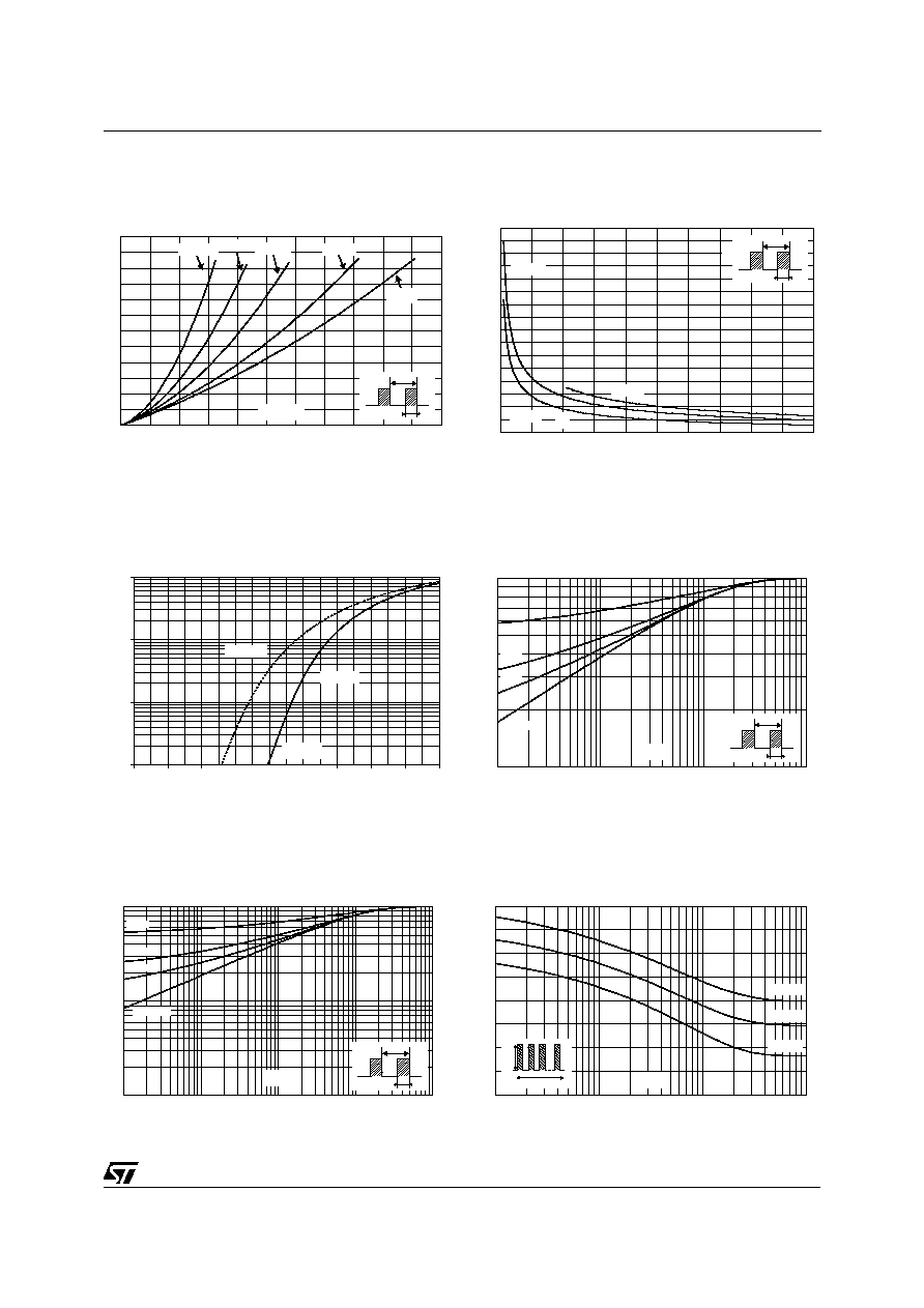
0
20
40
60
80
100
120
140
160
0.0
0.1
0.2
0.3
0.4
0.5
0.6
0.7
0.8
0.9
1.0
P = 10W
P = 5 W
P = 15W
T
=tp/T
tp
IM
IM(A)
Fig.2 : Peak current versus form factor.
0.1
1.0
10.0
100.0
0.0
0.2
0.4
0.6
0.8
1.0
1.2
1.4
1.6
1.8
VFM(V)
Tj=25įC
Tj=125įC
IFM(A)
Fig.3 : Forward voltage drop versus forward cur-
rent (maximum values).
0.1
1.0
1.E-03
1.E-02
1.E-01
1.E+00
tp(s)
T
=tp/T
tp
= 0.5
= 0.2
= 0.1
Single pulse
Zth(j-c)/Rth(j-c)
Fig.4-1 : Relative variation of thermal impedance
junction to case versus pulse duration (TO-220AC,
D
2
PAK).
0
2
4
6
8
10
12
0
1
2
3
4
5
6
7
8
9
10
11
IF(av)(A)
PF(av)(W)
= 0.05
= 0.1
= 0.2
= 0.5
= 1
T
=tp/T
tp
Fig.1 : Average forward power dissipation versus
average forward current.
0
10
20
30
40
50
60
70
80
1.E-03
1.E-02
1.E-01
1.E+00
t(s)
Tc=25įC
Tc=75įC
Tc=120įC
IM(A)
I
M
t
=0.5
Fig.5-1 : Non repetitive surge peak forward current
versus overload duration (TO-220AC, D
2
PAK).
0.0
0.1
1.0
1.E-03
1.E-02
1.E-01
1.E+00
1.E+01
tp(s)
Zth(j-c)/Rth(j-c)
T
=tp/T
tp
= 0.5
= 0.2
= 0.1
Single pulse
Fig.4-2 :Relative variation of thermal impedance
junction
to
case
versus
pulse
duration
(TO-220FPAC, ISOWATT220AC).

BYW29/F/FP/G-200
4/7
0
10
20
30
40
50
60
1.E-03
1.E-02
1.E-01
1.E+00
t(s)
Tc=25įC
Tc=75įC
Tc=100įC
IM(A)
I
M
t
=0.5
Fig.5-2 : Non repetitive surge peak forward cur-
rent versus overload duration (TO-220FPAC,
ISOWATT220AC).
0
1
2
3
4
5
6
7
8
9
10
0
25
50
75
100
125
150
Tamb(įC)
Rth(j-a)=Rth(j-c)
Rth(j-a)=15įC:W
TO-220AC/D≤PAK
TO-220FPAC
ISOWATT220AC
IF(av)(A)
Fig.6 : Average current versus ambient tempera-
ture. (
= 0.5)
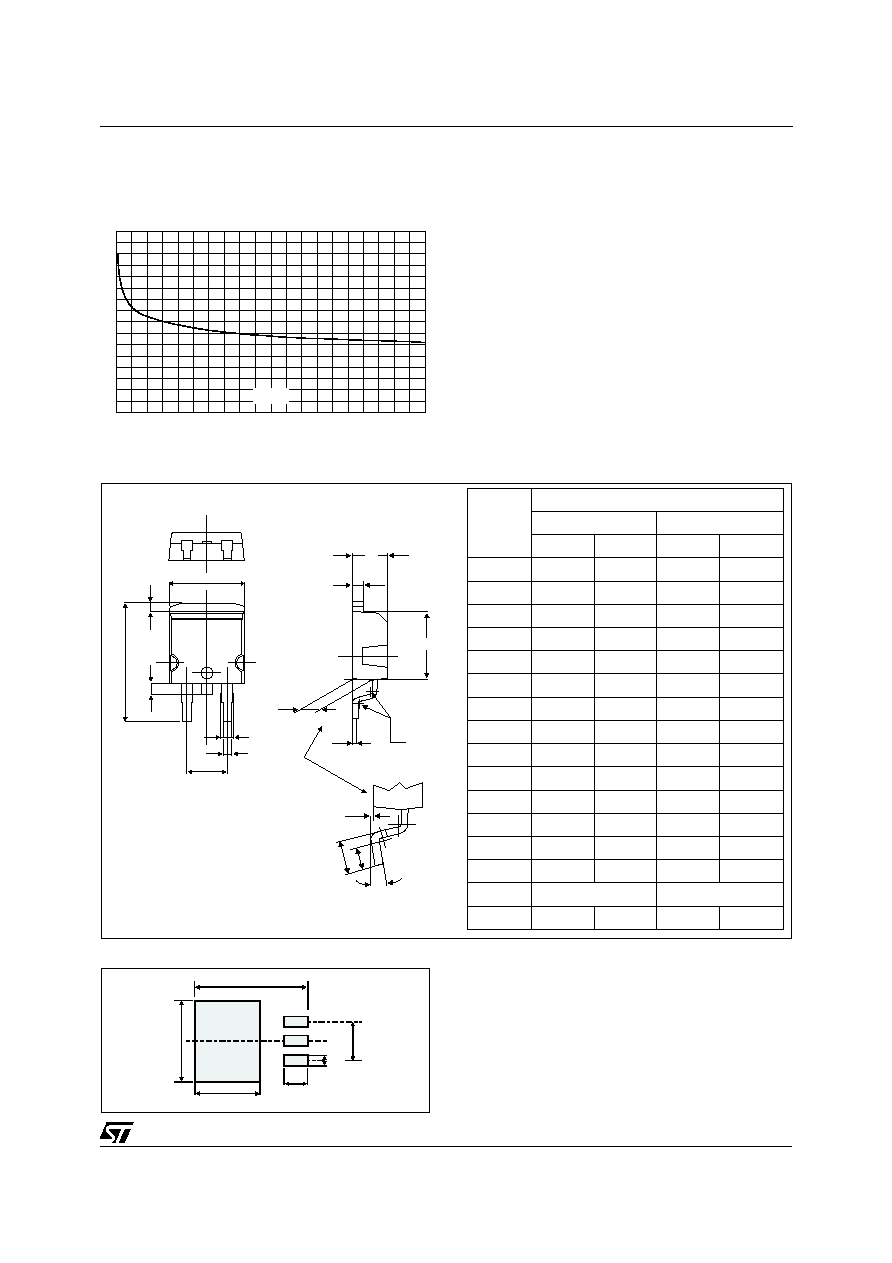
10
100
1000
10
100
1000
dIF/dt(A/Ķs)
IF=8A
VR=100V
Tj=100įC
Qrr(nC)
Fig.8 : Reverse recovery charges versus dI
F
/dt
(90%confidence).
10
100
1
10
100
1000
VR(V)
F=1MHz
Vosc=30mV
Tj=25įC
C(pF)
Fig.7 : Junction capacitance versus reverse volt-
age applied (Typical values).
1
10
100
10
100
1000
dIF/dt(A/Ķs)
IF=8A
VR=100V
Tj=100įC
IRM(A)
Fig.9 : Peak reverse recovery current versus
dIF/dt (90% confidence).
0.00
0.25
0.50
0.75
1.00
1.25
1.50
0
25
50
75
100
125
150
Tj(įC)
IRM
QRR
IF=8A
VR=100V
Qrr; IRM[Tj] / Qrr; IRM[Tj=125įC]
Fig.10 : Dynamic parameters versus junction tem-
perature.
5/7
BYW29/F/FP/G-200
PACKAGE MECHANICAL DATA
D
2
PAK (Plastic)
A
C2
D
R
A2
M
V2
C
A1
G
L
L3
L2
B
B2
E
*
* FLAT ZONE NO LESS THAN 2mm
REF.
DIMENSIONS
Millimeters
Inches
Min.
Max.
Min.
Max.
A
4.40
4.60
0.173
0.181
A1
2.49
2.69
0.098
0.106
A2
0.03
0.23
0.001
0.009
B
0.70
0.93
0.027
0.037
B2
1.14
1.70
0.045
0.067
C
0.45
0.60
0.017
0.024
C2
1.23
1.36
0.048
0.054
D
8.95
9.35
0.352
0.368
E
10.00
10.40
0.393
0.409
G
4.88
5.28
0.192
0.208
L
15.00
15.85
0.590
0.624
L2
1.27
1.40
0.050
0.055
L3
1.40
1.75
0.055
0.069
M
2.40
3.20
0.094
0.126
R
0.40 typ.
0.016 typ.
V2
0į
8į
0į
8į
8.90
3.70
1.30
5.08
16.90
10.30
FOOT PRINT (in millimeters)
0
10
20
30
40
50
60
70
80
0
2
4
6
8
10
12
14
16
18
20
S(cm≤)
Rth(j-a)(įC/W)
Fig.11 : Thermal resistance junction to ambient
versus copper surface under tab (Epoxy printed
circuit board FR4, copper thickness: 35Ķm) for
D
2
PAK.