June 2006
Rev 3
1/8
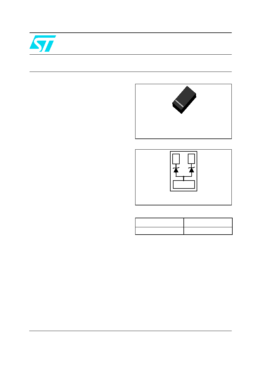
ESDALC6V1M3
Dual low capacitance TRANSILTM array for ESD protection
Main product applications
Where transient overvoltage protection in ESD
sensitive equipment is required, such as:
Computers
Printers
Communication systems
Cellular phone handsets and accessories
Video equipment
Features
2 unidirectional low capacitance TRANSIL
diodes
Breakdown Voltage V
BR
= 6.1 V min
Low diode capacitance (11 pF typ at 0 V)
Low leakage current < 0.5 µA
Very small PCB area: 0.6 mm²
RoHS compliant
Description
The ESDALC6V1M3 is a monolithic array
designed to protect 1 line or 2 lines against ESD
transients.
The device is ideal for applications where both
reduced line capacitance and board space saving
are required.
Benefits
High ESD protection level
High integration
Suitable for high density boards
TRANSIL is a trademark of STMicroelectronics
Configuration
Order code
Complies with the following standards
Part number
Marking
ESDALC6V1M3
K
IEC61000-4-2 level 4:
15 kV (air discharge)
8 kV (contact discharge)
MIL STD 883E-Method 3015-7: class 3
HBM (Human Body Model)
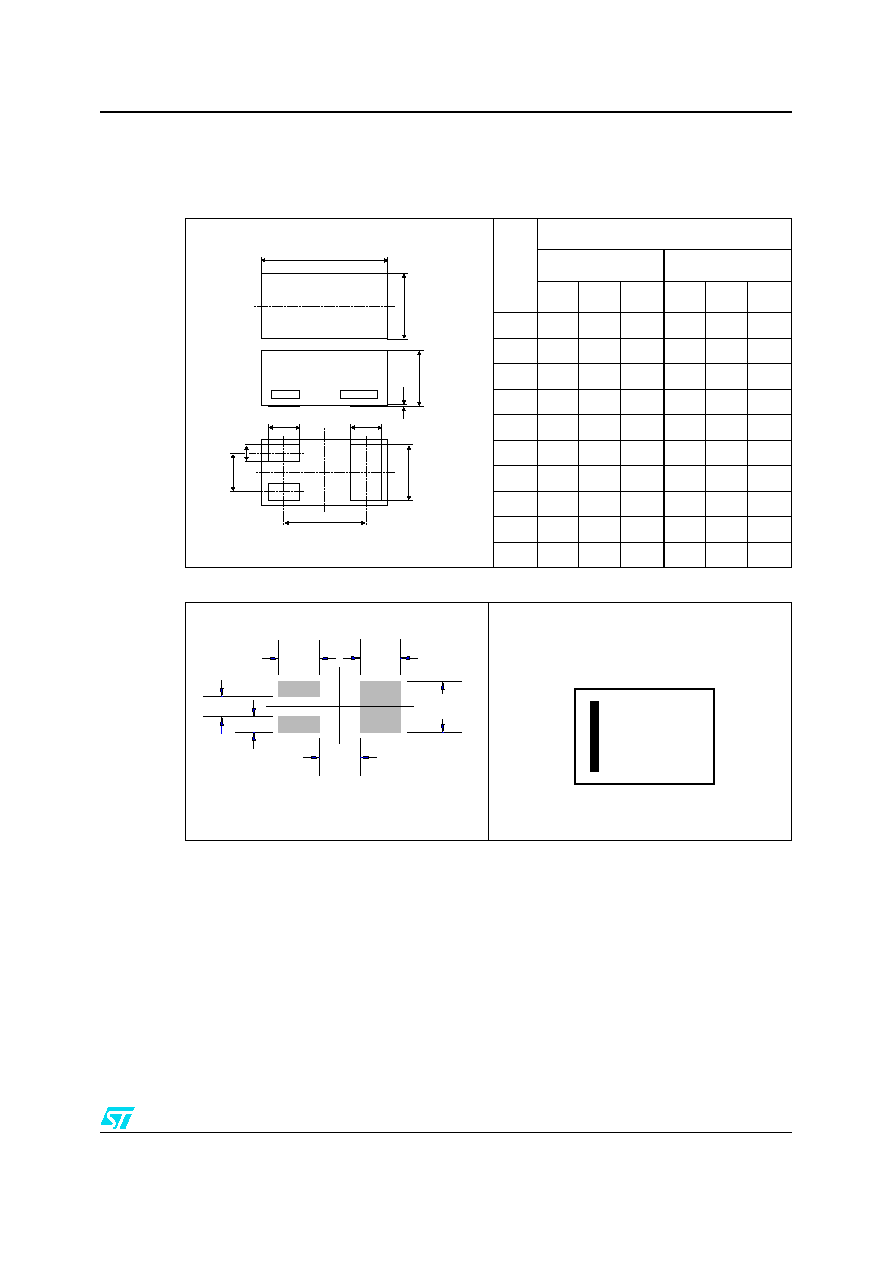
SOT 883
(JEDEC MO-236AA Compliant)
GND
GND
3
1
2
2
I/O2
GND
I/O1
GND
3
2
2
1
Underside view
www.st.com
Characteristics
ESDALC6V1M3
2/8
1 Characteristics
Table 1.
Absolute ratings (T
AMB
= 25° C - limiting values)
Symbol
Parameter
Value
Unit
V
PP
ESD discharge
IEC61000-4-2 air discharge
IEC61000-4-2 contact discharge
± 15
± 8
kV
P
PP
Peak pulse power dissipation (8/20 µs)
(1)
1.
For a surge greater than the maximum values, the diode will fail in short-circuit.
T
j
initial = T
AMB
30
W
I
pp
Repetitive peak pulse current (8/20 µs)
3
A
Tj
Junction temperature
125
° C
Tstg
Storage temperature range
-55 + 150
° C
T
L
Maximum lead temperature for soldering during 10 s
260
° C
T
OP
Operating temperature range
-40 + 125
° C
Table 2.
Electrical characteristics (T
AMB
= 25° C)
Symbol
Parameter
V
RM
Stand-off voltage
V
BR
Breakdown voltage
V
CL
Clamping voltage
I
RM
Leakage current @ V
RM
I
PP
Peak pulse current
T
Voltage temperature coefficient
V
F
Forward voltage drop
Parameter
Test condition
Min
Typ
Max
Unit
V
BR
I
R
= 1 mA
6.1
7.2
V
I
RM
V
RM
= 5 V
0.5
µA
R
d
1.1
T
I
R
= 1 mA
4.2
10
-4
/°C
C V
R
= 0 V, F = 1 MHz, V
OSC
= 30 mV
11
pF
V
V
V
I RM
I R
I PP
V
I
I F
V
V
Slope= 1/ Rd
V
V
CL
V
BR
RM
V
F
ESDALC6V1M3
Characteristics
3/8
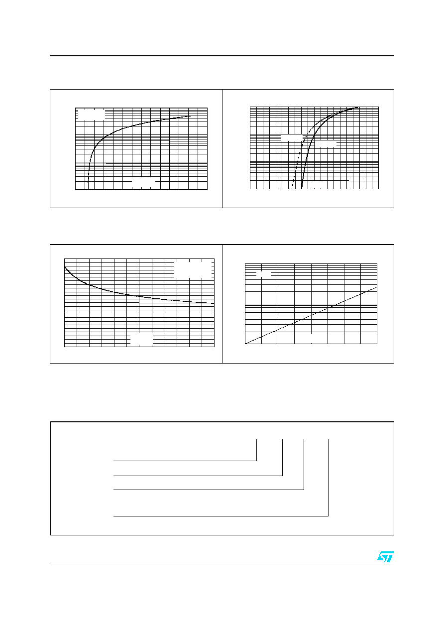
Figure 1.
S21 attenuation measurement
results of each channel
Figure 2.
Analog crosstalk measurements
between channels
100.0k
1.0M
10.0M
100.0M
1.0G
- 40.00
- 30.00
- 20.00
- 10.00
0.00
Att 1
1.8 GHz
540 MHz
- 3 dB
100.0k
1.0M
10.0M
100.0M
1.0G
- 40.00
- 30.00
- 20.00
- 10.00
0.00
Att 1
1.8 GHz
540 MHz
- 3 dB
f (Hz)
dB
100.0k
1.0M
10.0M
100.0M
1.0G
- 120.00
- 90.00
- 60.00
- 30.00
0.00
Xtalk
-52 dB
-9.3 dB
100.0k
1.0M
10.0M
100.0M
1.0G
- 120.00
- 90.00
- 60.00
- 30.00
0.00
Xtalk
-52 dB
-9.3 dB
dB
f (Hz)
Figure 3.
ESD response to IEC61000-4-2
(+15 kV air discharge) on each
channel
Figure 4.
ESD response to IEC61000-4-2
(-15 kV air discharge) on each
channel.
Figure 5.
Relative variation of peak pulse
power versus initial junction
temperature
Figure 6.
Peak pulse power versus
exponential pulse duration
0.0
0.1
0.2
0.3
0.4
0.5
0.6
0.7
0.8
0.9
1.0
1.1
0
25
50
75
100
125
150
PPP[Tj initial] /PPP[Tj initial=25°C]
Tj(°C)
10
100
1000
1
10
100
PPP(W)
tP(µs)
T initial = 25 °C
j
Ordering information scheme
ESDALC6V1M3
4/8
2
Ordering information scheme
Figure 7.
Clamping voltage versus peak
pulse current (typical values)
Figure 8.
Forward voltage drop versus peak
forward current (typical values)
0.1
1.0
10.0
100.0
0
10
20
30
40
50
60
70
IPP(A)
VCL(V)
8/20 µs
Tjinitial =25 °C
1.E-03
1.E-02
1.E-01
1.E+00
0.0
0.2
0.4
0.6
0.8
1.0
1.2
1.4
1.6
1.8
2.0
IFM(A)
V(V)
T
j
=125°C
T =25°C
j
Figure 9.
Junction capacitance versus
reverse voltage applied (typical
values)
Figure 10.
Relative variation of leakage
current versus junction
temperature (typical values)
0
1
2
3
4
5
6
7
8
9
10
11
12
0
1
2
3
4
5
6
C(pF)
F=1 MHz
VOSC = 30 mVRMS
Tj = 25 °C
VLINE (V)
VR = 3V
1
10
100
25
50
75
100
125
IR[Tj] / IR[Tj=25 °C]
T
j
(°C)
ESDA LC 6V1 M3
ESD Array
Low Capacitance
Package
M3 = SOT883
Breakdown Voltage
6V1 = 6.1 Volts min