1/9
ESDALC6V1W5
Æ
June 2002 - Ed: 4A
QUAD TRANSILTM ARRAY
FOR ESD PROTECTION
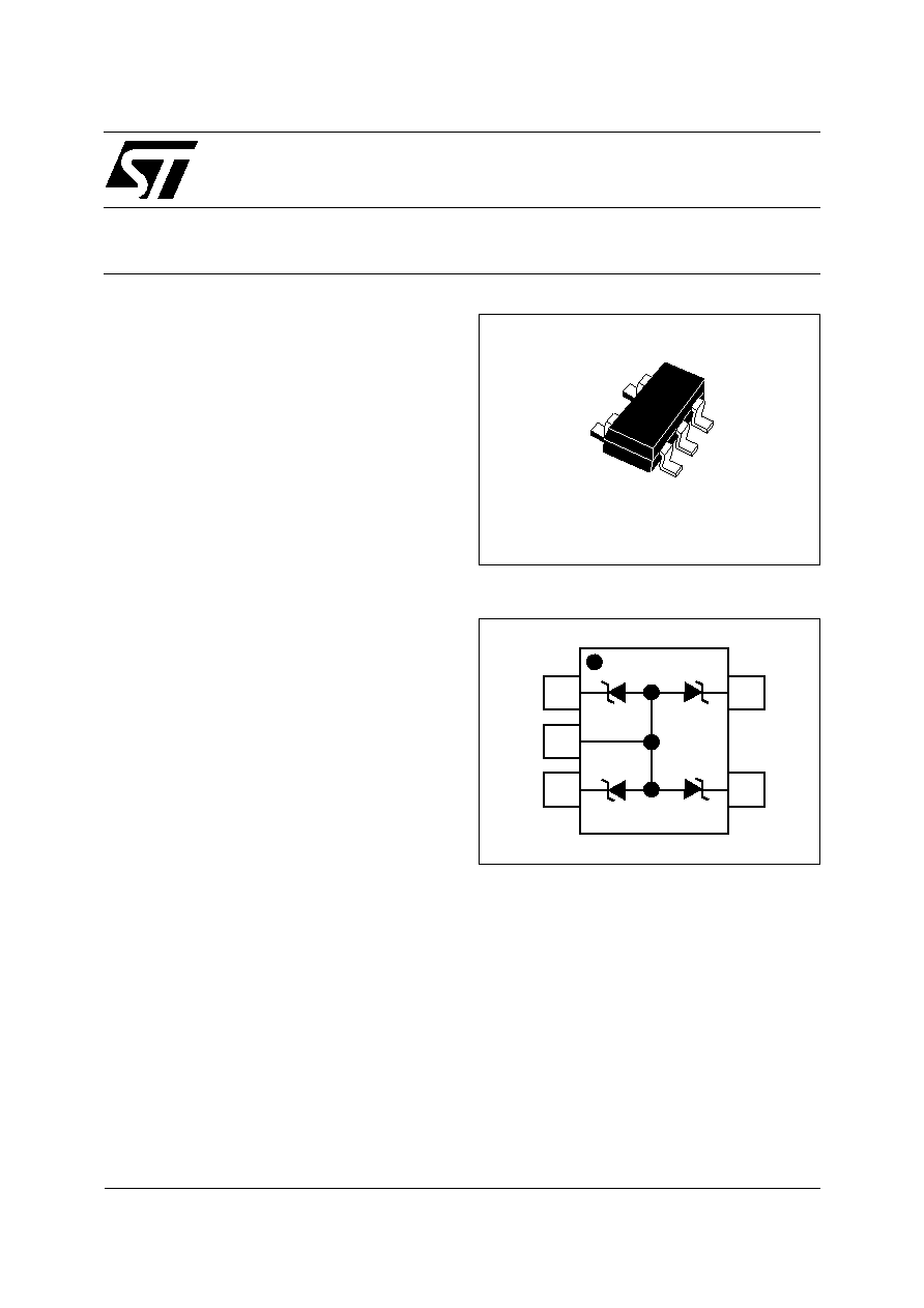
SOT323-5L
Where transient overvoltage protection in ESD
sensitive equipment is required, such as :
s
Computers
s
Printers
s
Communication systems and cellular phones
s
Video equipment
s
Set top boxes
MAIN APPLICATIONS
Application Specific Discretes
A.S.D.
I/01
I/02
GND
I/04
I/03
FUNCTIONAL DIAGRAM
s
4 unidirectional TRANSILTM functions.
s
ESD Protection: IEC61000-4-2 level 4
s
Breakdown voltage V
BR
= 6.1V min
s
Low leakage current < 1µA @ 3 Volts
s
Low capacitance device
FEATURES
The ESDALC6V1W5 is a 4-bit wide monolithic
suppressor which is designed to protect component
connected to data and transmission lines against
ESD.
It clamps the voltage just above the logic level
supply for positive transients, and to a diode drop
below ground for negative transients.
DESCRIPTION
s
High ESD protection level : up to 25 kV.
s
Capacitance: 12pF @ 0V Typ.
s
High integration.
s
Suitable for high density boards.
BENEFITS
s
IEC61000-4-2 level 4: 15 kV (air discharge)
8 kV (contact discharge)
s
MIL STD 883C-Method 3015-6 : class 3.
(human body model) 25kV (HBM)
COMPLIES WITH THE FOLLOWING STANDARDS :

ESDALC6V1W5
2/9
Symbol
Parameter
V
RM
Stand-off voltage
V
BR
Breakdown voltage
V
CL
Clamping voltage
I
RM
Leakage current
I
PP
Peak pulse current
C
Capacitance per line
Rd
Dynamic resistance
ELECTRICAL CHARACTERISTICS (T
amb
= 25∞C)
V
I
V
RM
PP
I
RM
I
V
BR
R
I
V
CL
slope : 1 / R
d
Symbol
Parameter
Test conditions
Value
Unit
V
PP
ESD discharge - MIL STD 883E - Method 3015-7
IEC61000-4-2 air discharge
IEC61000-4-2 contact discharge
± 25
± 15
± 8
kV
P
PP
Peak pulse power (8/20
µ
s)
25
W
T
j
Junction temperature
150
∞
C
T
stg
Storage temperature range
- 55 to + 150
∞C
T
op
Operating temperature range
- 40 to + 150
∞C
ABSOLUTE MAXIMUM RATINGS (T
amb
= 25∞C)
Types
V
BR
@
I
R
I
RM
@
V
RM
Rd
T
C
C
min.
max.
max.
typ.
max.
typ.
max.
note 1
note 2
3V bias
3V bias
V
V
mA
µ
A
V
m
10
-4
/∞C
pF
pF
ESDALC6V1W5
6.1
7.2
1
1
3
1100
6
7.5
9.5
Note 1 : Square pulse Ipp = 15A, tp=2.5
µ
s.
Note 2 :
VBR =
T* (Tamb -25∞C) * VBR (25∞C)
ESDALC6V1W5
3/9
0.0
0.1
0.2
0.3
0.4
0.5
0.6
0.7
0.8
0.9
1.0
1.1
0
25
50
75
100
125
150
175
Tj(∞C)
Ppp[Tj initial] / Ppp [Tj initial = 25∞C]
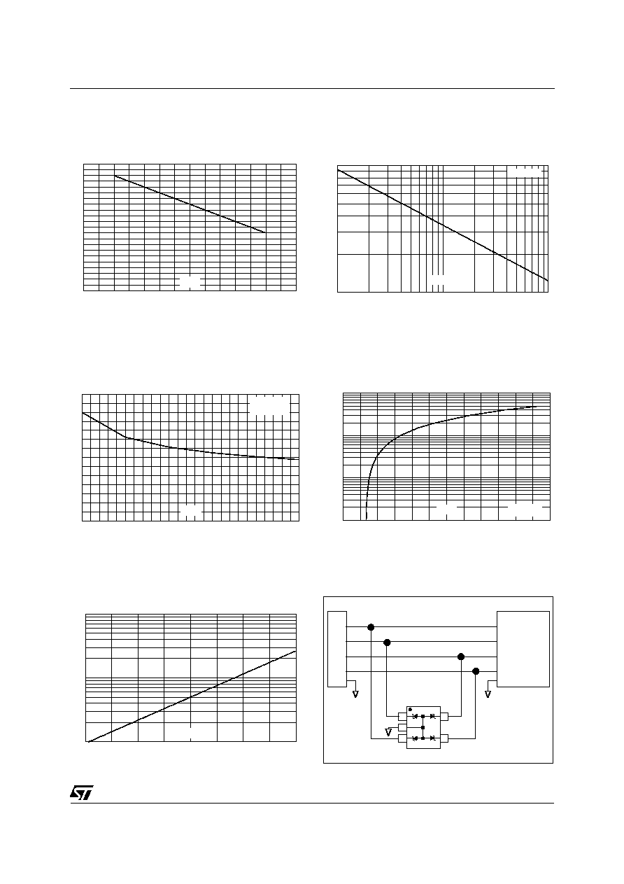
Fig. 1: Relative variation of peak pulse power
versus initial junction temperature.
10
100
1
10
100
tp(µs)
Tj initial = 25∞C
Ppp(W)
Fig. 2: Peak pulse power versus exponential pulse
duration.
0
2
4
6
8
10
12
14
0
1
2
3
4
5
VR(V)
F=1MHz
Vosc=30mV
RMS
Tj=25∞C
C(pF)
Fig. 3: Junction capacitance versus reverse voltage
applied (typical values).
0.1
1.0
10.0
100.0
0
10
20
30
40
50
60
Vcl(V)
tp=2.5µs
Tj initial =25∞C
Ipp(A)
Fig. 4: Clamping voltage versus peak pulse cur-
rent (maximum values, rectangular waveform).
1
10
100
25
50
75
100
125
Tj(∞C)
IR [Tj] / IR [Tj=25∞C]
Fig. 5: Relative variation of leakage current versus
junction temperature (typical values).
Connector
IC
to be
protected
I/02
I/01
I/04
I/03
Fig. 6: Application example
ESDALC6V1W5
4/9
With the focus of lowering the operation levels, the problem of malfunction caused by the environment is
critical. Electrostatic discharge (ESD) is a major cause of failure in electronic systems.
As a transient voltage suppressor, ESDALC6V1W5 is an ideal choice for ESD protection by suppressing
ESD events. It is capable of clamping the incoming transient to a low enough level such that any damage is
prevented on the device protected by ESDALC6V1W5.
ESDALC6V1W5 serves as a parallel protection elements, connected between the signal line and ground.
As the transient rises above the operating voltage of the device, the ESDALC6V1W5 becomes a low
impedance path diverting the transient current to ground.
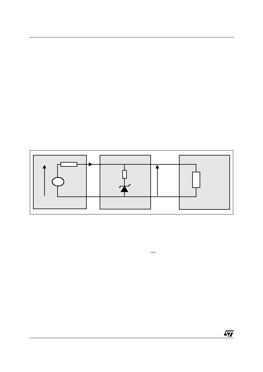
The clamping voltage is given by the following formula:
V
CL
= V
BR
+ Rd.I
PP
As shown in figure A1, the ESD strikes are clamped by the transient voltage suppressor.
1. ESD protection by ESDALC6V1W5
TECHNICAL INFORMATION
Rd
R
G
V
G
V
BR
V(i/o)
R
L O
AD
Device
to be
protected
ESD surge
ESDALC6V1W5
I
PP
Fig. A1: ESD clamping behavior
To have a good approximation of the remaining voltages at both Vi/o side, we provide the typical dynamical
resistance value Rd. By taking into account the following hypothesis:
Rg > Rd and Rload > Rd
we have:
( )
V i o
V
R
V
R
BR
d
g
g
/
=
+
◊
The results of the calculation done Vg = 8kV, Rg = 330
(IEC61000-4-2 standard), V
BR
= 6.1V (min) and
Rd = 1.1
(typ.) give:
( )
V i o
Volts
/
,
=
32 8
This confirms the very low remaining voltage across the device to be protected. It is also important to note
that in this approximation the parasitic inductance effect was not taken into account. This could be a few
tenths of volts during a few ns at the Vi/o side.
ESDALC6V1W5
5/9
V(i/o)
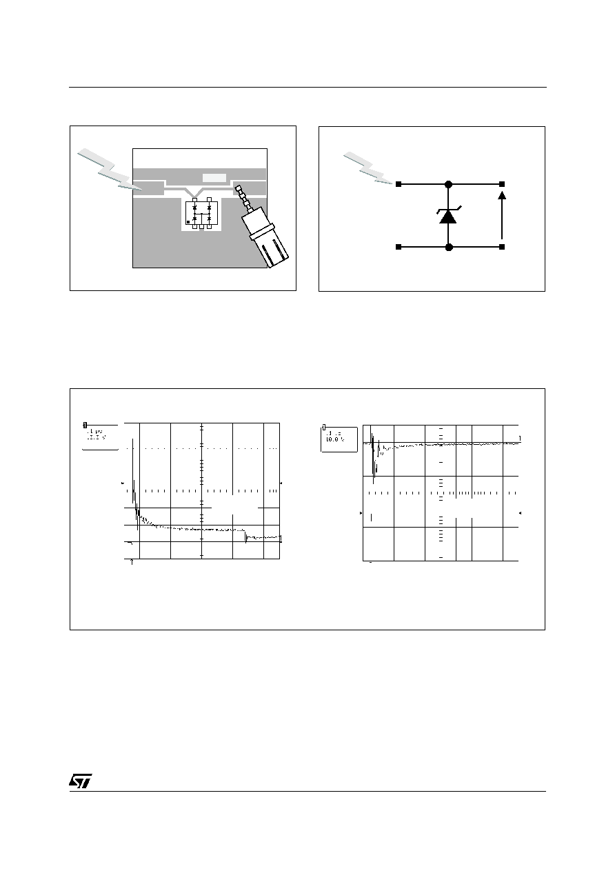
TEST BOARD
V(i/o)
Fig. A2: ESD test board
B2
I/O1, I/O2, I/O3 or I/O4
V(i/o)
± 8kV
ESD Contact
discharge
Fig. A3: ESD test configuration
The measurements done here after show very clearly (Fig. A4) the high efficiency of the ESD protection:
the clamping voltage V(i/o) becomes very close to +V
BR
(positive way, Fig. A4a) and -V
BR
(negative way,
Fig. A4b).
Fig. A4: Remaining voltage during ESD surge
V(i/o)
V(i/o)
a: Response in the positive way
b: Response in the negative way