1/11
October 2002
s
32 TIMES STANDARD B-SERIES OUTPUT
CURRENT DRIVE SINKING CAPABILITY -
136 mA TYP. AT V
DD
= 10V, V
DS
= 1V
s
QUIESCENT CURRENT SPECIF. UP TO 20V
s
5V, 10V AND 15V PARAMETRIC RATINGS
s
INPUT LEAKAGE CURRENT
I
I
= 100nA (MAX) AT V
DD
= 18V T
A
= 25∞C
s
100% TESTED FOR QUIESCENT CURRENT
s
MEETS ALL REQUIREMENTS OF JEDEC
JESD13B "STANDARD SPECIFICATIONS
FOR DESCRIPTION OF B SERIES CMOS
DEVICES"
DESCRIPTION
HCF40107B is a monolithic integrated circuit
fabricated in Metal Oxide Semiconductor
technology available in DIP and SOP packages.
HCF40107B is a dual 2-input NAND buffer/driver
containing two independent 2-input NAND buffers
with open-drain single n-channel transistor
outputs. This device features a wired-OR
capability and high output sink current capability
(136 mA typ. at V
DD
= 10V, V
DS
= 1V).
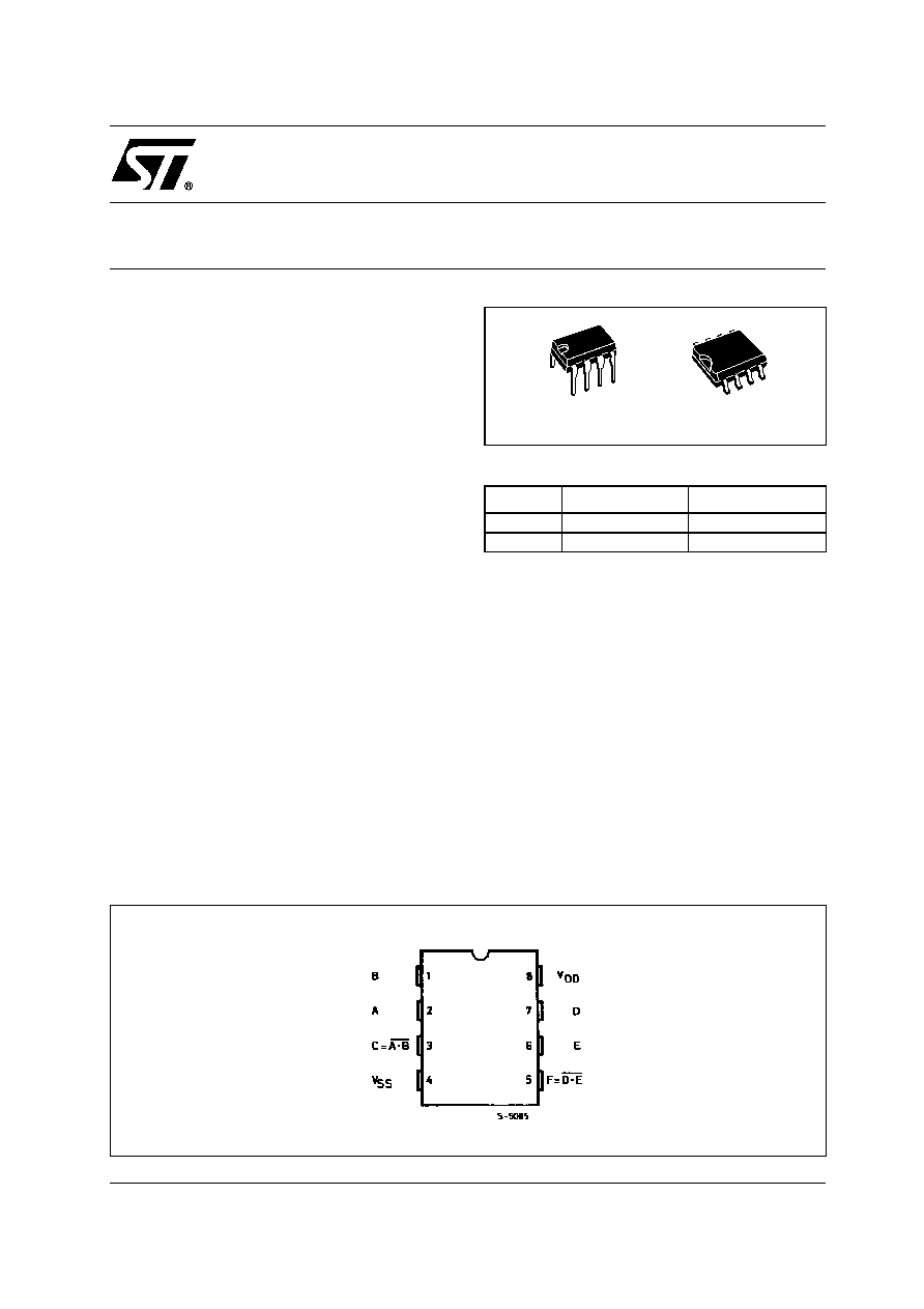
HCF40107B
DUAL 2-INPUT NAND BUFFER/DRIVER
PIN CONNECTION
ORDER CODES
PACKAGE
TUBE
T & R
DIP
HCF40107BEY
SOP
HCF40107BM1
HCF40107M013TR
DIP
SOP
HCF40107B
2/11
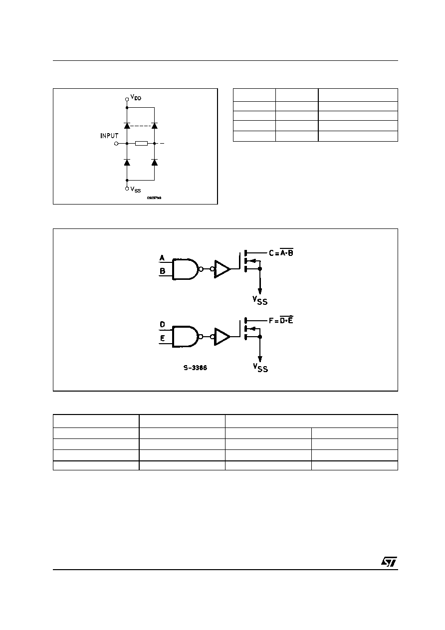
INPUT EQUIVALENT CIRCUIT
PIN DESCRIPTION
FUNCTIONAL DIAGRAM
TRUTH TABLE
* : Requires external and pull-up resistor (R
L
) to V
DD
.
# : Without pull-up resistor (3-state).
PIN No
SYMBOL
NAME AND FUNCTION
2, 1, 7, 6
A, B, D, E
Input
3, 5
C,F
Outputs
4
V
SS
Negative Supply Voltage
8
V
DD
Positive Supply Voltage
A
B
C
L
L
H*
Z
#
H
L
H*
Z
#
L
H
H*
Z
#
H
H
L

HCF40107B
3/11
LOGIC DIAGRAM
ABSOLUTE MAXIMUM RATINGS
Absolute Maximum Ratings are those values beyond which damage to the device may occur. Functional operation under these conditions is
not implied.
All voltage values are referred to V
SS
pin voltage.
RECOMMENDED OPERATING CONDITIONS
Symbol
Parameter
Value
Unit
V
DD
Supply Voltage
-0.5 to +22
V
V
I
DC Input Voltage
-0.5 to V
DD
+ 0.5
V
I
I
DC Input Current
±
10
mA
P
D
Power Dissipation per Package
200
mW
Power Dissipation per Output Transistor
100
mW
T
op
Operating Temperature
-55 to +125
∞C
T
stg
Storage Temperature
-65 to +150
∞C
Symbol
Parameter
Value
Unit
V
DD
Supply Voltage
3 to 20
V
V
I
Input Voltage
0 to V
DD
V
T
op
Operating Temperature
-55 to 125
∞C

HCF40107B
4/11
DC SPECIFICATIONS
The Noise Margin for both "1" and "0" level is: 1V min. with V
DD
=5V, 2V min. with V
DD
=10V, 2.5V min. with V
DD
=15V
** Measured with external pull-up resistor, R
L
= 10k
to V
DD
.
*** Forced output disabled.
DYNAMIC ELECTRICAL CHARACTERISTICS (T
amb
= 25∞C, C
L
= 50pF, R
L
= 200K
, t
r
= t
f
= 20 ns)
(*) R
L
is external pull-up resistor to V
DD.
Symbol
Parameter
Test Condition
Value
Unit
V
I
(V)
V
O
(V)
|I
O
|
(
µ
A)
V
DD
(V)
T
A
= 25∞C
-40 to 85∞C
-55 to 125∞C
Min.
Typ.
Max.
Min.
Max.
Min.
Max.
I
L
Quiescent Current
0/5
5
0.02
5
150
30
µ
A
0/10
10
0.02
10
300
60
0/15
15
0.02
20
600
120
0/20
20
0.04
100
3000
600
V
IH**
High Level Input
Voltage
0.5/4.5
<1
5
3.5
3.5
3.5
V
1/9
<1
10
7
7
7
1.5/13.5
<1
15
11
11
11
V
IL**
Low Level Input
Voltage
4.5/0.5
<1
5
1.5
1.5
1.5
V
9/1
<1
10
3
3
3
13.5/1.5
<1
15
4
4
4
I
OL
Output Sink
Current
5
0.4
5
21
32
16
12
mA
5
1
5
44
68
30
25
10
0.5
10
49
74
37
28
10
1
10
89
136
68
51
15
0.5
15
66
100
50
38
I
OH
Output Drive
Current
No Internal Pull-up Device
mA
I
IH,
I
IL
Input Leakage
Current
0/18
Any Input
18
±
10
-5
±
0.1
±
0.1
±
1
µ
A
I
OH,
I
OL
***
3-State Output
Leakage Current
0/18
18
18
±
10
-4
2
2
20
µ
A
C
I
Input Capacitance
Any Input
5
7.5
pF
C
O
Output
Capacitance
Any Output
30
pF
Symbol
Parameter
Test Condition
Value (*)
Unit
V
DD
(V)
Min.
Typ.
Max.
t
PHL
t
PLH
Propagation Delay Time
High to Low
5
R
L
* = 120
100
200
ns
10
45
90
15
30
60
Low to High
5
R
L
* = 120
100
200
ns
10
60
120
15
50
100
t
THL
t
TLH
Transition Time
High to Low
5
R
L
* = 120
50
100
ns
10
20
40
15
10
20
Low to High
5
R
L
* = 120
50
100
ns
10
35
70
15
25
50
HCF40107B
5/11
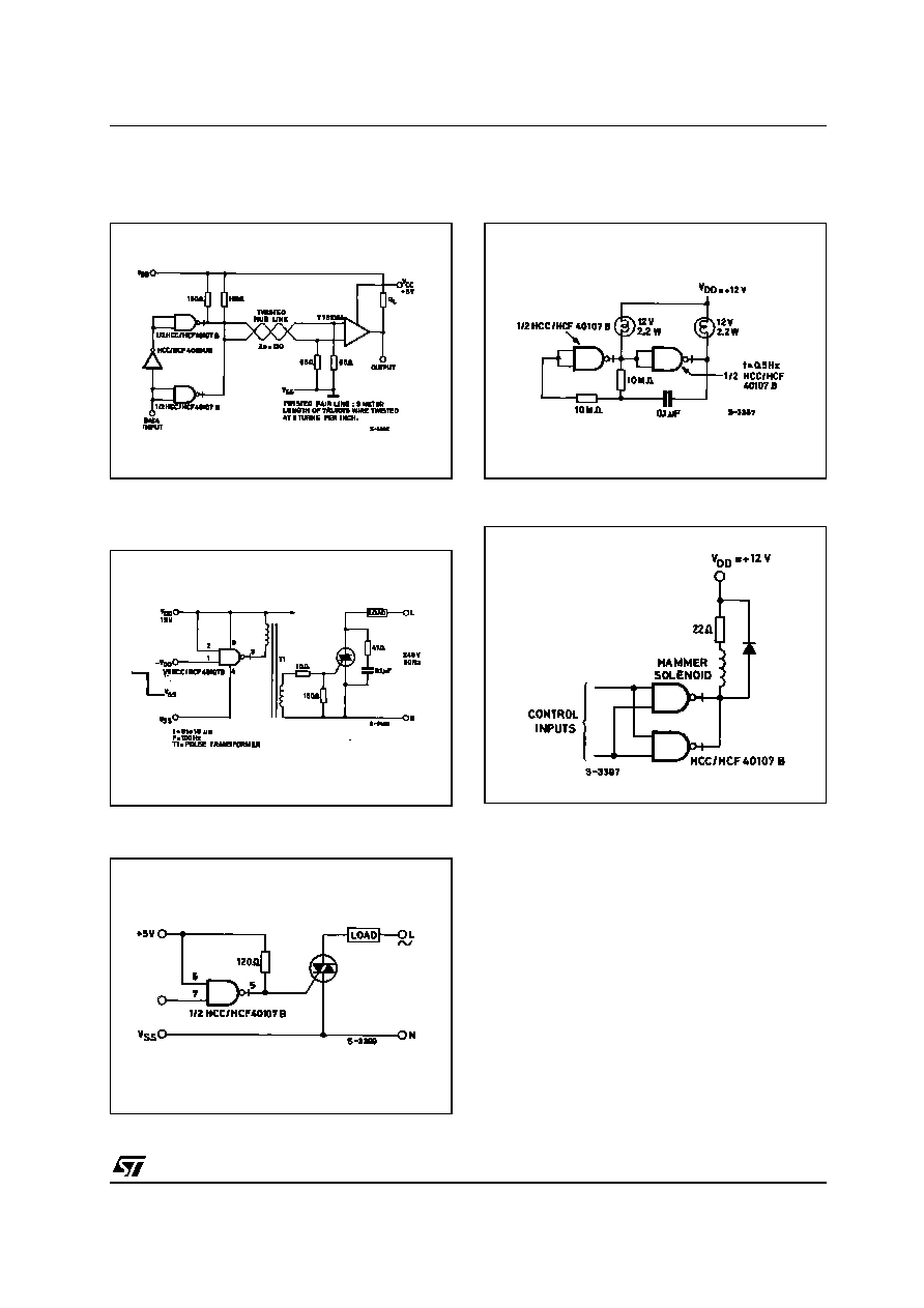
TYPICAL APPLICATIONS
Line-driver Circuit.
Interface of 40107B with Triac, with COS/MOS
Component and Triac isolated.
Direct Dc Driver Interface of 40107B with a Triac.
A 2.2-watt Incandescent Lamp-driver Circuit.
Solenoid Driver Circuit