 | –≠–ª–µ–∫—Ç—Ä–æ–Ω–Ω—ã–π –∫–æ–º–ø–æ–Ω–µ–Ω—Ç: IRF640T | –°–∫–∞—á–∞—Ç—å:  PDF PDF  ZIP ZIP |
October 2006
Rev 1
1/12
12
Extremely high dv/dt capability
Gate charge minimized
Very low intrinsic capacitances
Description
This Power MOSFET is designed using the
company's consolidated strip layout-based MESH
OVERLAYTM process. This technology matches
and improves the performances compared with
standard parts from various sources.
Applications
Switching application
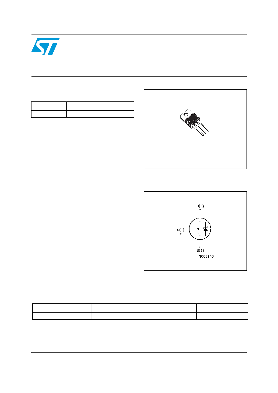
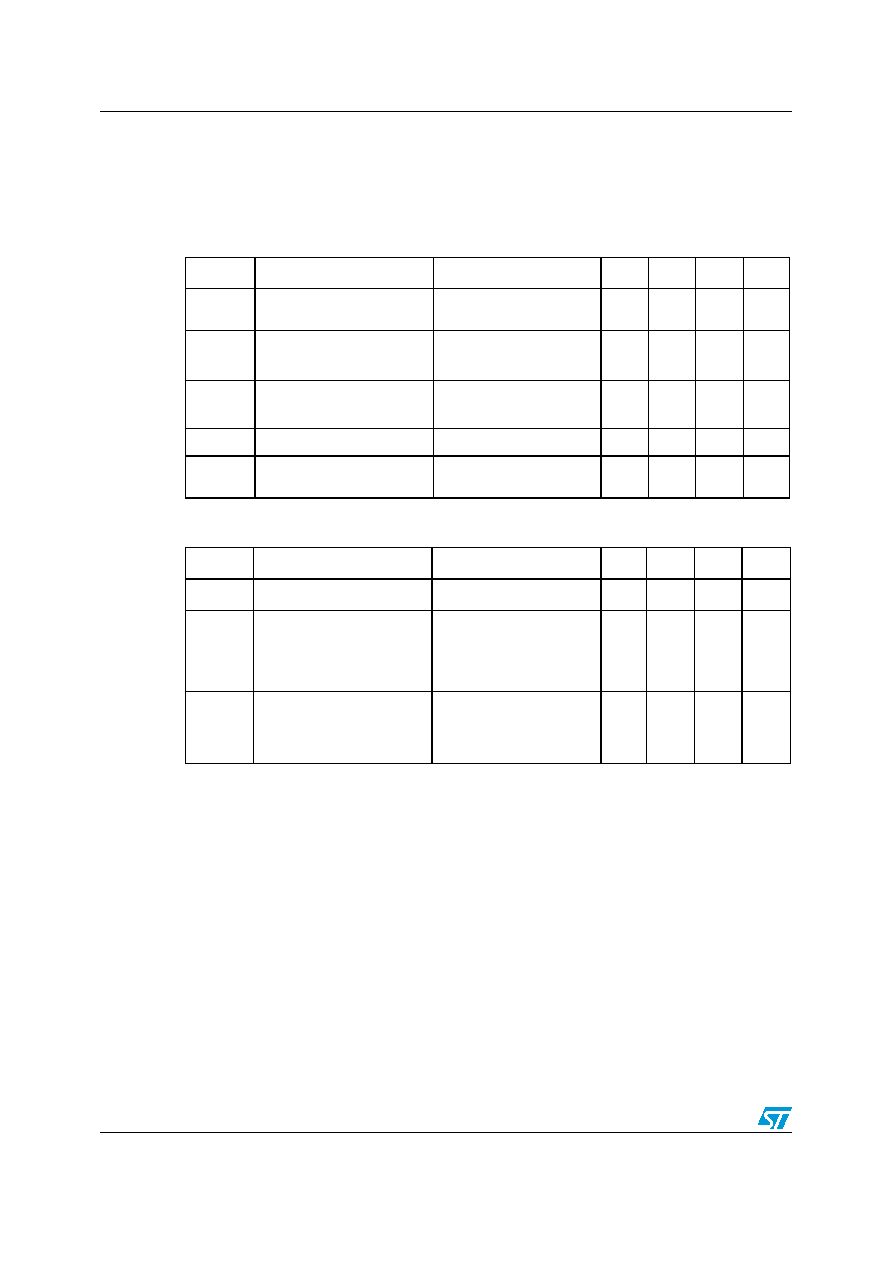
Internal schematic diagram
General features
Type
V
DSS
R
DS(on)
I
D
IRF640T
200V
<0.16
15A
1
2
3
TO-220
IRF640T
N-channel 200V - 0.15
- 15A - TO-220
MESH OVERLAYTM Power MOSFET
www.st.com
Order codes
Part number
Marking
Package
Packaging
IRF640T
IRF640T
TO-220
Tube

Contents
IRF640T
2/12
Rev 1
Contents
1
Electrical ratings . . . . . . . . . . . . . . . . . . . . . . . . . . . . . . . . . . . . . . . . . . . . 3
2
Electrical characteristics . . . . . . . . . . . . . . . . . . . . . . . . . . . . . . . . . . . . . 4
2.1
Electrical characteristics (curves) . . . . . . . . . . . . . . . . . . . . . . . . . . . . . 6
3
Test circuit . . . . . . . . . . . . . . . . . . . . . . . . . . . . . . . . . . . . . . . . . . . . . . . . 8
4
Package mechanical data . . . . . . . . . . . . . . . . . . . . . . . . . . . . . . . . . . . . . 9
5
Packaging mechanical data . . . . . . . . . . . . . . . . . . . . . . . . . . . . . . . . . . 12
6
Revision history . . . . . . . . . . . . . . . . . . . . . . . . . . . . . . . . . . . . . . . . . . . 13

IRF640T
Electrical ratings
Rev 1
3/12
1 Electrical
ratings
Table 1.
Absolute maximum ratings
Symbol
Parameter
Value
Unit
V
DS
Drain-source voltage (V
GS
= 0)
200
V
V
GS
Gate-source voltage
± 20
V
I
D
Drain current (continuous) at T
C
= 25∞C
15
A
I
D
Drain current (continuous) at T
C
=100∞C
10
A
I
DM
(1)
1.
Pulse width limited by safe operating area
Drain current (pulsed)
60
A
P
TOT
Total dissipation at T
C
= 25∞C
90
W
Derating factor
0.72
W/∞C
dv/dt
(2)
2.
I
SD
15A, di/dt
300A/µs, V
DD
=80%
V
(BR)DSS
Peak diode recovery voltage slope
15
V/ns
T
J
T
stg
Operating junction temperature
Storage temperature
-55 to 150
∞C
Table 2.
Thermal data
Symbol
Parameter
Value
Unit
R
thj-case
Thermal resistance junction-case max
1.38
∞C/W
R
thj-a
Thermal resistance junction-ambient max
62.5
∞C/W
T
l
Maximum lead temperature for soldering purpose
300
∞C
Table 3.
Avalanche data
Symbol
Parameter
Value
Unit
I
AR
Avalanche curent, repetitive or not-repetitive
(pulse width limited by Tj Max)
15
A
E
AS
Single pulse avalanche energy
(starting Tj=25∞C, Id=Iar, Vdd=50V)
110
mJ
Electrical characteristics
IRF640T
4/12
Rev 1
2 Electrical
characteristics
(T
CASE
=25∞C unless otherwise specified)
Table 4.
On/off states
Symbol
Parameter
Test conditions
Min.
Typ.
Max.
Unit
V
(BR)DSS
Drain-source breakdown
voltage
I
D
= 1mA, V
GS
= 0
200
V
I
DSS
Zero gate voltage drain
current (V
GS
= 0)
V
DS
= Max rating,
V
DS
= Max rating @125∞C
1
10
µA
µA
I
GSS
Gate body leakage current
(V
DS
= 0)
V
GS
= ±20V
±
100
nA
V
GS(th)
Gate threshold voltage
V
DS
= V
GS
, I
D
= 250µA
2
3
4
V
R
DS(on)
Static drain-source on
resistance
V
GS
= 10V, I
D
= 7.5A
0.15
0.16
Table 5.
Dynamic
Symbol
Parameter
Test conditions
Min.
Typ.
Max.
Unit
g
fs
(1)
1.
Pulsed: pulse duration=300µs, duty cycle 1.5%
Forward transconductance
V
DS
=8V, I
D
= 7.5A
12
S
C
iss
C
oss
C
rss
Input capacitance
Output capacitance
Reverse transfer
capacitance
V
DS
=25V, f=1 MHz,
V
GS
=0
800
165
26
pF
pF
pF
Q
g
Q
gs
Q
gd
Total gate charge
Gate-source charge
Gate-drain charge
V
DD
=160V, I
D
= 15A
V
GS
=10V
(see Figure 14)
24
4.4
11.6
nC
nC
nC
IRF640T
Electrical characteristics
Rev 1
5/12
Table 6.
Switching times
Symbol
Parameter
Test conditions
Min.
Typ.
Max.
Unit
t
d(on)
t
r
Turn-on delay time
Rise time
V
DD
=100 V, I
D
= 7.5A,
R
G
=4.7
, V
GS
=10V
(see Figure 13)
11.5
22
ns
ns
t
d(off)
t
f
Turn-off delay time
Fall time
V
DD
= 100 V, I
D
= 7.5A,
R
G
= 4.7
, V
GS
= 10V
(see Figure 13)
19
11
ns
ns
Table 7.
Source drain diode
Symbol
Parameter
Test conditions
Min
Typ.
Max
Unit
I
SD
Source-drain current
15
A
I
SDM
(1)
1.
Pulse width limited by safe operating area
Source-drain current (pulsed)
60
A
V
SD
(2)
2.
Pulsed: pulse duration = 300µs, duty cycle 1.5%
Forward on voltage
I
SD
=15A, V
GS
=0
1.6
V
t
rr
Q
rr
I
RRM
Reverse recovery time
Reverse recovery charge
Reverse recovery current
I
SD
=15A, V
DD
=50V
di/dt = 100A/µs,
(see Figure 18)
125
0.55
8.8
ns
µC
A
t
rr
Q
rr
I
RRM
Reverse recovery time
Reverse recovery charge
Reverse recovery current
I
SD
=15A, V
DD
=50V
di/dt = 100A/µs,
Tj=150∞C
(see Figure 18)
148
0.73
9.9
ns
µC
A