 | –≠–Ľ–Ķ–ļ—ā—Ä–ĺ–Ĺ–Ĺ—č–Ļ –ļ–ĺ–ľ–Ņ–ĺ–Ĺ–Ķ–Ĺ—ā: ITA10B3 | –°–ļ–į—á–į—ā—Ć:  PDF PDF  ZIP ZIP |

ITA6V5B3 / ITA10B3
ITA18B3 / ITA25B3
ģ
January 1998 Ed: 2
BIDIRECTIONAL TRANSIL
TM
ARRAY
FOR DATALINE PROTECTION
SO20
Differential data transmission lines protection :
- RS-232
- RS-423
- RS-422
- RS-485
APPLICATIONS
Application Specific Discretes
A.S.D.
TM
FUNCTIONAL DIAGRAM
HIGH SURGE CAPABILITY TRANSIL ARRAY
I
PP
= 40 A (8/20
Ķ
s)
PEAK PULSE POWER : 300 W (8/20
Ķ
s)
SEPARATED INPUT-OUTPUT
UP TO 9 BIDIRECTIONAL TRANSIL FUNCTIONS
LOW CLAMPING FACTOR (V
CL
/ V
BR
) AT HIGH
CURRENT LEVEL
LOW LEAKAGE CURRENT
ESD PROTECTION UP TO 15kV
FEATURES
DESCRIPTION
Transil diode arrays
provide high overvoltage
protectionby clamping action. Their instantaneous
response to transient overvoltages makes them
particularly suited to protect voltage sensitive
devices such as MOS Technology and low voltage
supplied IC's.
The ITA series allies high surge capability against
energetic pulses with high voltage performance
against ESD.
The separated input/output configuration of the
device ensures improved protection against very
fast transient overvoltage like ESD by elimination
of the spikes induced by parasitic inductances
created by external wiring.
IEC 1000-4-2 : level 4
IEC 1000-4-4 : level 4
IEC 1000-4-5 : level 2
MIL STD 883C - Method 3015-6 : class 3
(human body model)
COMPLIESWITH THE FOLLOWINGSTANDARDS :
1/6

Symbol
Parameter
V
RM
Stand-off voltage
V
BR
Breakdown voltage
V
CL
Clamping voltage
I
RM
Leakage current @ V
RM
I
PP
Peak pulse current
T
Voltage temperature coefficient
C
Junction capacitance
ELECTRICAL CHARACTERISTICS (T
amb
= 25
į
C)
Symbol
Parameter
Value
Unit
P
PP
Peak pulse power dissipation (8/20
Ķ
s)
(see note 1)
Tj initial = T
amb
300
W
I
PP
Peak pulse current (8/20
Ķ
s) (see note 1)
Tj initial = T
amb
40
A
I
2
t
Wire I
2
t value (see note 1)
0.6
A
2
s
T
stg
T
j
Storage temperature range
Maximum operating junction temperature
- 55 to + 150
125
į
C
į
C
T
L
Maximum lead temperature for soldering during 10s
260
į
C
ABSOLUTE MAXIMUM RATINGS (T
amb
= 25
į
C)
100
50
0
20
s
t
%I
pp
8 s
Pulse wave form 8/20 s
Types
I
RM
@
V
RM
V
BR
@
I
R
V
CL
@
I
PP
V
CL
@
I
PP
T
C
max.
min.
8/20
Ķ
s
max.
8/20
Ķ
s
max.
max.
note 2
note 2
note 2
note 3
Ķ
A
V
V
mA
V
A
V
A
10
-4
/
į
C
pF
ITA6V5B3
10
5
6.5
1
9.5
10
11
25
4
1100
ITA10B3
4
8
10
1
13
10
17
25
8
800
ITA18B3
4
15
18
1
21
10
26
25
9
500
ITA25B3
4
24
25
1
31
10
36
25
12
420
Note 2 : Between I/O pin and ground.
Note 3 : Between two input Pins at 0V Bias.
Preferred types in bold.
Note 1 : For surges greater than the specified maximum
value, the I/O will first present a short-circuit and after an
open circuit caused by the wire melting.
ģ
ITA6V5B3 / ITA10B3 / ITA18B3 / ITA25B3
2/6

P
(W)
1E-03
1E-02
1E-01
1E+00
1E+01
1E+02
1E+01
1E+02
1E+03
1E+04
P
T
initial = 25 C
o
j
t
(ms) expo
P
ITA25B3
ITA18B3
ITA10B3
ITA6V5B3
P
Fig. 1 : Typical peak pulse power versus
exponential pulse duration.
I
(A)
1E-02
1E-01
1E+00
1E+01
1E+00
1E+01
1E+02
1E+03
DC
expon ential waveform
t (ms)
Fig. 3 : Peak current I
DC
inducing open circuit of
the wire for one input/output versus pulse duration
(typical values).
Fig. 4 : Junction capacitance versus reverse
applied voltage for one input/output (typical
values).
Fig.
2 : Clamping voltage versus peak pulse
current (exponential waveform 8/20
Ķ
s).
Fig. 5 : Relative variation of leakage current
versus junction temperature
ģ
ITA6V5B3 / ITA10B3 / ITA18B3 /ITA25B3
3/6

This monolithic Transil Array is based on 10
unidirectional Transils with a commoncathode and
can be configurated to offer up to 9 bidirectional
functions. This imposes a maximum differential
voltage between 2 input pins (see opposite table).
Types
Maximum differential voltage
between two input pins at 25
į
C
ITA6V5B3
+ / - 3.5 V
ITA10B3
+ / - 5.0 V
ITA18B3
+ / - 9.0 V
ITA25B3
+ / - 12.5 V
APPLICATION INFORMATION
Typical application : RS232 junction.
CARRIER DET.
GND
CTS
RTS
TX
RX
AUX
DSR
DTR
ģ
ITA6V5B3 / ITA10B3 / ITA18B3 / ITA25B3
4/6
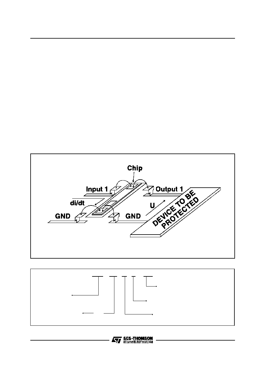
Design advantage of ITAxxxB3 used with 4-point structure.
The ITAxxxB3 has been designed with a 4-point structure (separated Input/output) in order to efficiently
protect against disturbances with very high di/dt rates, such as ESD.
The purpose of this 4-point structure is to eliminate the overvoltage introduced by the parasitic inductances
of the wiring (Ldi/dt).
Efficient protection depends not only on the component itself, but also on the circuit layout.The drawing
given in figure shows the layout to be used in order to take advantage of the 4-point structure of the
ITAxxxB3.
With this layout, each line to be protected passes through the protection device.
In this way, it realizes an interface between the data line and the circuit to be protected, guaranteeing an
isolation between its inputs and outputs.
APPLICATION NOTICE
The 4 - point structure layout.
ORDER CODE
ITA
25 B 3
RL
INTEGRATED
TRANSIL ARRAY
V
BR
min
PACKAGE : SO20 PLASTIC
BIDIRECTIONAL
PACKAGING:
RL = Tape and reel.
= Tube.
ģ
ITA6V5B3 / ITA10B3 / ITA18B3 /ITA25B3
5/6