 | –≠–ª–µ–∫—Ç—Ä–æ–Ω–Ω—ã–π –∫–æ–º–ø–æ–Ω–µ–Ω—Ç: ITAxxB1 | –°–∫–∞—á–∞—Ç—å:  PDF PDF  ZIP ZIP |

Æ
1/6
ITAxxB1
BIDIRECTIONAL TRANSILTM ARRAY
FOR DATALINE PROTECTION
REV. 1
SO-8
December 2004
MAIN APPLICATIONS
Differential data transmission lines protection,
such as :
RS-232
RS-423
RS-422
RS-485
FEATURES
High surge capability Transil array:
I
PP
= 40 A (8/20µs)
Peak pulse power : 300 W (8/20µs)
Up to 5 bidirectional Transil functions
Low clamping factor (V
CL
/ V
BR
) at high current
level
Low leakage current
ESD protection up to 15kV
DESCRIPTION
Transil diode arrays provide high overvoltage pro-
tection by clamping action. Their instantaneous re-
sponse to transient overvoltages makes them
particularly suited to protect voltage sensitive de-
vices such as MOS Technology and low voltage
supplied IC's.
The ITA series combines high surge capability
against energetic pulses with high voltage per-
formance against ESD.
COMPLIES WITH THE FOLLOWING STANDARDS:
IEC61000-4-2 level 4:
15kV (air discharge)
8kV
(contact discharge)
MIL STD 883E-Method 3015-7: class3
25kV HBM (Human Body Model)
Table 1: Order Codes
Part Number
Marking
ITA6V5B1
6V5B1
ITA6V5B1RL
6V5B1
ITA10B1
10B1
ITA18B1
18B1
ITA18B1RL
18B1
ITA25B1
25B1
ITA25B1RL
25B1
ASDTM
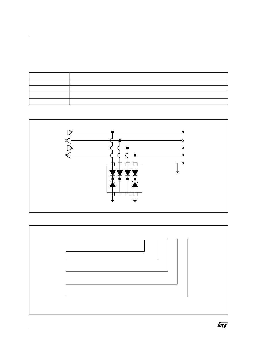
Figure 1: Functional Diagram
1
2
3
4
I/O1
I/O2
I/O3
I/O4
GND
GND
8
7
6
5
TM: ASD and TRANSIL are trademarks of STMicroelectronics.

ITAxxB1
2/6
Table 2: Absolute Ratings (T
amb
= 25∞C)
Table 3: Electrical Characteristics (T
amb
= 25∞C)
Symbol
Parameter
Value
Unit
P
PP
Peak pulse power (8/20µs) (see note 1)
T
j
initial = T
amb
300
W
I
PP
Peak pulse current (8/20µs) (see note 1)
T
j
initial = T
amb
40
A
I
2
t
Wire I
2
t value (see note 1)
0.6
A
2
s
T
j
Maximum operating junction temperature
125
∞C
T
stg
Storage temperature range
-55 to +150
∞C
T
L
Maximum lead temperature for soldering during 10 s at 5mm for case
260
∞C
Note 1: For surges greater than the specified maximum value, the I/O will first present a short-circuit and after an open circuit caused by
the wire melting.
Symbol
Parameter
V
RM
Stand-off voltage
V
BR
Breakdown voltage
V
CL
Clamping voltage
I
RM
Leakage current
I
PP
Peak pulse current
T
Voltage temperature coefficient
V
F
Forward voltage drop
C
Capacitance
Part Number
V
BR
@ I
R
I
RM
@ V
RM
V
CL
@ I
PP
V
CL
@ I
PP
T
C
min.
max.
8/20µs
max.
8/20µs
max.
max.
note 2
note 2
note 2
note 3
V
mA
µA
V
V
A
V
A
10
-4
/∞C
pF
ITA6V5B1
6.5
1
10
5
10
10
12
25
4
750
ITA10B1
10
1
4
8
15
10
19
25
8
570
ITA18B1
18
1
4
15
25
10
28
25
9
350
ITA25B1
25
1
4
24
33
10
38
25
12
300
Note 2: Between I/O pin and ground.
Note 3: Between two input pins at 0V Bias, F = 1 MHz.
V
BR
V
CL
V
RM
I
RM
I
PP
I
V

ITAxxB1
3/6
Figure 2: Pulse waveform
Figure 3: Typical peak pulse power versus
exponential pulse duration
Figure 4: Clamping voltage versus peak pulse
current (exponential waveform 8/20µs)
Figure 5: Peak current I
DC
inducing open
circuit of the wire for one input/output versus
pulse duration (typical values)
Figure 6: Junction capacitance versus reverse
applied voltage for one input/output (typical
values)
Figure 7: Relative variation of leakage current
versus junction temperature
%I
PP
t
10µs
100
50
0
1000µs
Pulse waveform 10/1000µs
P
PP
(W)
1E-03
1E-02
1E-01
1E+00
1E+01
1E+02
1E+01
1E+02
1E+03
1E+04
T
j
initial=25∞C
t
P
(ms) expo
ITA18B1
ITA25B1
ITA6V5B1
ITA10B1
V
CL
(V)
T
j
initial=25∞C
I
PP
(A)
1E+00
1E+01
1E+02
1E+03
1E-01
1E+00
1E+01
1E+02
ITA18B1
ITA25B1
ITA6V5B1
ITA10B1
%I
PP
t
r
100
50
0
t
p
t
I
DC
(A)
t
P
(ms)
1E+00
1E+01
1E+02
1E+03
1E-02
1E-01
1E+00
1E+01
Exponential waveform
C(pF)
T
j
=25∞C
F=1MHz
V
R
(V)
1E+02
1E+03
1E+00
1E+01
1E+02
ITA18B1
ITA25B1
ITA6V5B1
ITA10B1
5E+3
1E+3
1E+2
1E+1
0
25
50
75
100
125
150
1E+0
1E-1
T
j
(∞C)
I
R
(T )
I (T =25∞C)
j
R
j
V
R
=V
RM
ITAxxB1
4/6
This monolithic Transil Array is based on 6 unidirectional Transils with a common cathode and can be con-
figurated to offer up to 5 bidirectional functions. This imposes a maximum differential voltage between 2
input pins (see table 4).
Table 4: Application information
Figure 8: RS-232 junction (typical application)
Figure 9: Ordering Information Scheme
Types
Maximum differential voltage between two input pins at 25∞C
ITA6V5B1
+ / - 3.5 v
ITA10B1
+ / - 5.0 v
ITA18B1
+ / - 9.0 v
ITA25B1
+ / - 12.5 v
GND
CTS
RTS
TX
RX
ITA 25 B 1 RL
Integrated Transil Array
Breakdown Voltage (min)
Type of lines protected
Package
Packaging
25 = 25 Volt
B = Bidirectional
1 = SO-8
RL = Tape & reel
Blank = Tube

ITAxxB1
5/6
Figure 10: SO-8 Package Mechanical Data
Figure 11: Foot Print Dimensions (in millimeters)
E
D
8
4
1
5
H
k
h x 45∞
L
C
(Seating
Plane)
0.25mm
(Gage Plane)
e
A
A2
B
A1
ddd C
6.8
4.2
1.27
0.6
Table 5: Ordering Information
Part Number
Marking
Package
Weight
Base qty
Delivery mode
ITA6V5B1
6V5B1
SO-8
0.08 g
2000
Ammopack
ITA6V5B1RL
6V5B1
2500
Tape & reel
ITA10B1
10B1
2000
Ammopack
ITA18B1
18B1
2000
Ammopack
ITA18B1RL
18B1
2500
Tape & reel
ITA25B1
25B1
2000
Ammopack
ITA25B1RL
25B1
2500
Tape & reel
Table 6: Revision History
Date
Revision
Description of Changes
13-Dec-2004
1
First issue
REF.
DIMENSIONS
Millimetres
Inches
Min.
Typ. Max. Min.
Typ. Max.
A
1.75
0.069
a1
0.1
0.25 0.004
0.010
a2
1.65
0.065
a3
0.65
0.85 0.025
0.033
b
0.35
0.48 0.014
0.019
b1
0.19
0.25 0.007
0.010
C
0.25
0.50
0.50 0.010
0.020
c1
45∞ (typ)
D
4.8
5.0
0.189
0.197
E
5.8
6.2
0.228
0.244
e
1.27
0.050
e3
3.81
0.150
F
3.8
4.0
0.15
0.157
L
0.4
1.27 0.016
0.050
M
0.6
0.024
S
8∞ (max)