 | –≠–ª–µ–∫—Ç—Ä–æ–Ω–Ω—ã–π –∫–æ–º–ø–æ–Ω–µ–Ω—Ç: LCP3121 | –°–∫–∞—á–∞—Ç—å:  PDF PDF  ZIP ZIP |

Application Specific Discretes
A.S.D.
TM
LCP3121
OVERVOLTAGE AND OVERCURRENT
PROTECTION FOR TELECOM LINE
Æ
UNIDIRECTIONAL
OVERVOLTAGE
SUP-
PRESSOR PROGRAMMABLE BY VOLTAGE
AND CURRENT:
PROGRAMMABLE BREAKDOWN VOLTAGE
UP TO 100 V.
PROGRAMMABLE
CURRENT
LIMITATION
FROM 120 mA TO 600 mA.
MULTI-LINE PROTECTION MODE : ONE DE-
VICE CAN PROTECT SEVERAL LINES.
HIGH SURGE CURRENT CAPABILITY :
I
PP
= 100A for 10/1000
µ
s.
FEATURES AND BENEFITS
SO8
Dedicated to the protection of sensitive telecom
equipment, the LCP3121 provides protection
which can be programmed by both voltage and
current.
The breakdown voltage can be easily programmed
by using an external zener diode.
The protection functionprogrammed by the current
is achieved with the use of a resistor between the
gate and the cathode. The value of the resistor will
determine the level of the desired current before
the triggering of the device.
A multiple protection mode is also performed when
using several diodes providing each line interface
with an optimized protection level.
If desired, a bidirectionalprotection functioncan be
achieved by the use of two LCP3121.
DESCRIPTION
September 1998 - Ed: 3
FUNCTIONAL DIAGRAM
A
Gp
C
Gn
CCITT K20 :
10/700
µ
s
1kV
5/310
µ
s
25A
VDE 0433 :
10/700
µ
s
2kV
5/310
µ
s
50A
VDE 0878 :
1.2/50
µ
s
1.5kV
1/20
µ
s
40A
FCC part 68 :
2/10
µ
s
2.5kV
2/10
µ
s
200A (*)
BELLCORE
TR-NWT-001089 :
2/10
µ
s
2.5kV
2/10
µ
s
200A (*)
BELLCORE
TR-NWT-000974 :
10/1000
µ
s
1kV
10/1000
µ
s
100A
(*) with series resistors or PTC.
COMPLIESWITH THE FOLLOWINGSTANDARDS :
PIN-OUT CONFIGURATION
1
2
3
4
5
6
7
8
C
Gn
Gp
A
A
C
C
C
All cathod pins must be externally connected
TM: ASD is trademarks of SGS-THOMSON Microelectronics.
1/6
Symbol
Parameter
Value
Unit
I
PP
Peak pulse current (see note 1)
10/1000
µ
s
100
A
I
TSM
Non repetitive surge peak on-state current
(F = 50 Hz)
t
p
= 10ms
t = 1s
16
8
A
V
AC
V
GA
Maximum voltage between A and C
Maximum voltage between G (Gn or Gp) and A
100
80
V
T
stg
T
j
Storage temperature range
Maximum junction temperature
- 40 to + 150
150
∞
C
T
L
Maximum lead temperature for soldering during 10s
260
∞
C
ABSOLUTE MAXIMUM RATINGS ( T
amb
= 25
∞
C)
Note 1 : Pulse waveform :
10/1000
µ
s
tr=10
µ
s
tp=1000
µ
s
100
50
% I
PP
t
t
r
p
0
t
Symbol
Parameter
Value
Unit
R
th (j-a)
Junction to ambient
170
∞
C/W
THERMAL RESISTANCE
Symbol
Parameter
V
RM
Stand-off voltage
V
BR
Breakdown voltage
V
BO
Breakover voltage
I
H
Holding current
I
BO
Breakover current
I
RM
Leakage current at V
RM
I
R
Leakage current at V
R
I
PP
Peak pulse current
V
R
Continuous reverse voltage
C
off
Off-state capacitance
V
G
Gate voltage
I
GP
Gp triggering current
I
GN
Gn triggering current
ELECTRICAL CHARACTERISTICS (T
amb
= 25
∞
C)
V
RM
I
H
PP
I
I
RM
V
BR
I
BO
V
BO
V
R
I
R
LCP3121
2/6
Symbol
Test conditions
Min.
Max.
Unit
V
G
note1
IGATE = 200mA (for eigher Gn or Gp)
0.6
1.8
V
I
GP
V
Anode-cathode
= 60V
180
mA
I
GN
V
Anode-cathode
= 60V
80
200
mA
Note 1 : VG = VGN, measured between Gn and cathode
VG = VGP, measured between Gp and anode
2 - OPERATION WITH GATE (T
amb
= 25
∞
C)
Symbol
Test conditions
Min.
Max.
Unit
I
RM
V
RM
= 60V
V
RM
= 90V
5
8
µ
A
I
R
at VR = 180V
50
µ
A
V
BR
at 1mA
100
V
I
BO
80
500
mA
V
BO
Measured at 50Hz
180
V
I
H
See the functional test circuit
100
mA
C
V
R
=-5V
F=1MHz
100
pF
1 - OPERATION WITHOUT GATE (T
amb
= 25
∞
C)
LCP3121
3/6
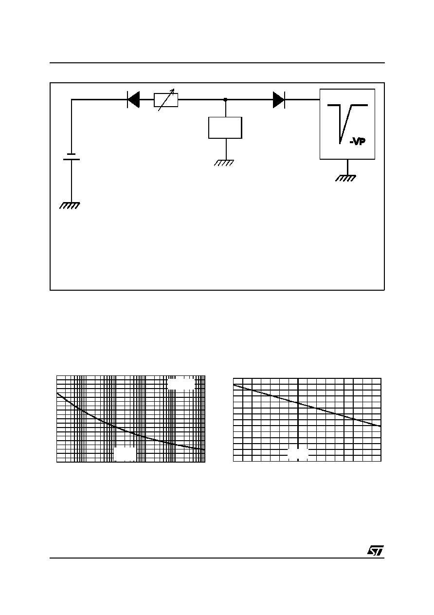
FUNCTIONAL HOLDING CURRENT (I
H
) TEST CIRCUIT : GO-NO GO TEST
0.01
0.10
1
10
100
1000
0
2
4
6
8
10
12
14
16
18
20
I
TSM
(A)
t(s)
F=50Hz
Tj initial = 25
∞
c
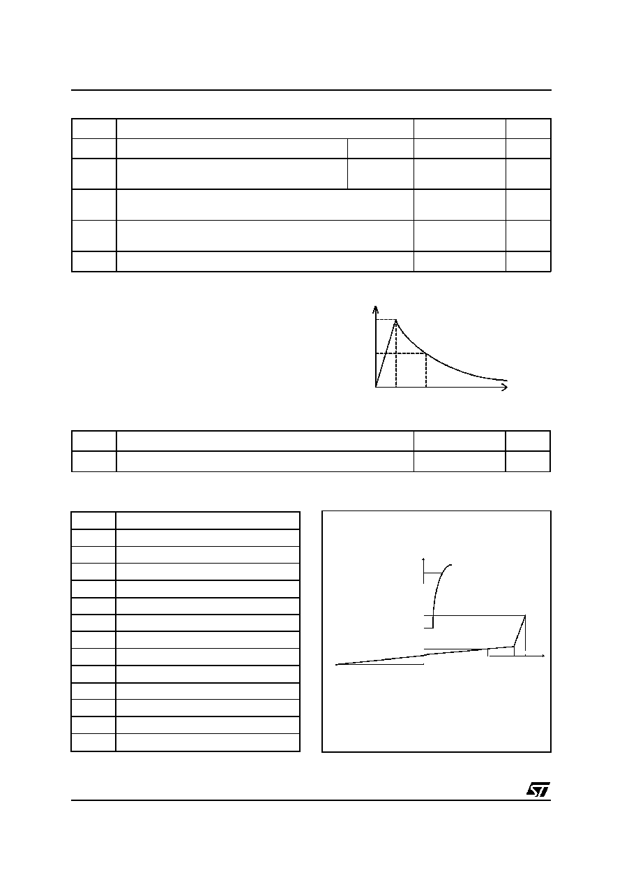
Fig. 1 : Maximum non repetitive surge peak-on-
state current versus overload duration.
-40
-20
0
20
40
60
80
100
120
0.0
0.2
0.4
0.6
0.8
1.0
1.2
1.4
Tj(
∞
C)
IH [Tj] / IH [Tj=25
∞
C]
Fig. 2 : Relative variation of holding current versus
junction temperature (typical values).
This is a GO-NO GO test which allows to confirm the holding current (I
H
) level in a functional test circuit.
TEST PROCEDURE :
- Adjust the current level at the I
H
value by short circuiting the D.U.T.
- Fire the D.U.T. with a surge current : I
PP
= 10A, 10/1000
µ
s.
- The D.U.T. will come back to the off-state within a duration of 50ms max.
R
Surge
generator
V
= -48 V
BAT
-V
P
D.U.T
LCP3121
4/6

Application 1 : Common protection for SLIC
without integrated ring generator
SLIC
LCP 3121
4*SMBYW01-200
-Vbat
TIP
RING
SLIC
4*SMBYW01-200
-Vbat
TIP
RING
-Vbat
Gn
C
A
APPLICATION EXAMPLES
Application 2 : Common protection for SLIC with
integrated ring generator
LCP3121
4*SMBYW01-200
TIP
RING
-Vbat
Gn
C
A
-Vbat +Vbat
LCP3121
+Vbat
Gp
C
A
SLIC
L3000N
4*SMBYW01-200
TIP
RING
-Vbat +Vbat
SLIC
L3000N
Application 3 : Typical SLIC protection
4*SMBYW01-200
-Vbat
-Vbat
SLIC
A
Gn
LCP3121
C
TIP
RING
Application 4 : Protection programmed by current
LCP3121
A
C
Gn
Protec ted
Circuit
+
-
Ra
I = I
+
T
G
V
G
Ra
I
T
CURRENT TOLERANCE
R
a
(+/-5%)
I
T
mA
min
I
T
mA
max
4.7
5.6
6.8
8.2
10
12
202
182
164
150
137
128
603
538
479
431
388
358
LCP3121
5/6